


Samsung Securities 2025 Semiconductor Outlook (20250210)
A Must-Read Report for Tech Enthusiasts

Key Factor 1. Can Earnings Forecasts Be Revised Upward?
For companies with high exposure to general-purpose semiconductors, it will likely be difficult for earnings forecasts to be revised upward in the short term. In an effort to accelerate the cycle recovery, the supply industry is strongly controlling general-purpose semiconductor production. In this environment, it is challenging to be certain that Capex and utilization rate forecasts have bottomed out.
The market will want to see more concrete evidence of a cycle recovery going forward. Only when such evidence becomes visible will traditional semiconductor equipment and materials investment ideas—such as expectations of a Capex and utilization rate bottom-out—start being further reflected in stock prices. At this point, we believe that companies with high exposure to AI semiconductors have the upper hand in terms of earnings visibility and the potential for earnings revisions.
When Will Evidence of Improvement in General-Purpose Semiconductors Appear?
According to our projections, more concrete evidence of a general-purpose semiconductor cycle recovery (such as customer inventory normalization and the visible effects of supply reductions) is expected to emerge in May–June 2025. As this timeline approaches, expectations for a bottom-out in Capex and utilization rates could also gain further traction.
• Preconditions for Cycle Improvement: A key prerequisite for cycle improvement is the normalization of customer inventories. Once customer inventories return to normal, the rebound in general-purpose semiconductor purchases will become more tangible. Historically, the stock market has reacted more strongly to demand recovery opportunities than to supply reductions.
• The Winter Phase: We expect demand weakness to be inevitable from Q4 2024 to early Q2 2025. Even considering seasonal slowdowns, the Q1 2025 sales guidance recently provided by major memory semiconductor companies was weaker than expected. As customers have already secured sufficient inventory, they have little incentive to build additional stock, and they are likely to focus on digesting their existing inventory during this period.
• Signs of a Rebound: A positive aspect is that a sharp increase in supply chain inventories appears unlikely. For DRAM, the impact of high-bandwidth memory (HBM) capacity encroachment is expected to limit production increases in the first half of the year. For NAND, given the past restraint in front-end process investments, it will be difficult for production to surge. If inventory levels in the supply industry do not rise sharply during a period of weak demand, opportunities for a rebound could emerge sooner than expected.
• When Will the Effects of Supply Reduction Appear? Supply is just as important as demand in determining semiconductor market dynamics. The supply industry is estimated to be aggressively controlling production to expedite cycle recovery. Given that the lead time for memory semiconductors is typically around four months, if wafer input was reduced in January, the impact should become apparent by May. Once supply reductions become visible, customers may begin to shift their stance. Some may adopt a strategy of purchasing before prices rise significantly, which could shift bargaining power back from customers to suppliers.
• When Will Customer Inventory Normalize? Considering supply-demand changes, we expect customer inventory to begin normalizing around May–June 2025. Since purchasing plans for general-purpose semiconductors have been significantly reduced in recent months, we anticipate seeing signs of a recovery in purchasing from that period onward. As a result, expectations for a bottom-out in Capex and utilization rate forecasts could also begin to gain momentum in line with this timeline.
Key Factor 2. How Will Semiconductor Technology Change in 2025?
If semiconductor manufacturers’ Capex and utilization rates serve as short-term profit factors for the semiconductor equipment and materials industry, then the response to technological changes becomes a key determinant in valuing semiconductor equipment and materials stocks. Timely adaptation to technological changes is essential to create future growth drivers, and the stock market has always priced in future value in advance. Therefore, it is necessary to examine which technologies will be applied in 2025.
1. DRAM 1c Will Emerge in the First Half
DRAM 1c is expected to appear in the first half of 2025. One of the key technological changes to be emphasized is High‑K Metal Gate. With the growing need for technology that enables faster AI processing while consuming less power, High‑K Metal Gate is viewed as the core technology to achieve this. Although this technology has been applied mainly in mobile and graphics applications until now, it is expected to extend across all applications.
Looking at the process steps in detail, the following changes are anticipated:
1. Lithography:
• The number of EUV layers is expected to expand further. Micron Technology, which has not previously used EUV, is anticipated to introduce EUV starting with DRAM 1c. Similarly, Samsung Electronics and SK Hynix are expected to increase the number of EUV layers compared to DRAM 1b, thereby controlling the increase in lithography process steps and seizing opportunities for performance improvements.
• High‑NA EUV is not expected to be utilized until DRAM 1c. Although pre‑development for DRAM 1d is underway and may eventually incorporate High‑NA EUV, maximizing its utility will require prior upgrades in materials and components. Given that High‑NA EUV demands significantly higher source power compared to the existing Low‑NA EUV, further improvements in the durability of materials and components are presumed necessary.
2. Etching:
• With the expanded use of EUV leading to a more controlled increase in lithography process steps, the growth in the number of etching process steps is also expected to be more constrained compared to the past.
• However, as etching must be performed on increasingly finer scales, there remains an opportunity for ASP (Average Selling Price) increases driven by specification upgrades.
3. Deposition:
• There is an increasing need to form thinner and more uniform films to enhance integration density. This environment may lead to an increased number of ALD (Atomic Layer Deposition) process steps.
• Additionally, for existing CVD (Chemical Vapor Deposition) equipment, the proportion of Single‑Type systems—which can deposit films more uniformly than Batch‑Type systems—is expected to rise.
2. AI Memory Semiconductors: Spreading Optimism and Diversifying Product Lines
1. HBM:
• HBM4 is expected to emerge in the second half of 2025. From a process technology standpoint, the following changes are anticipated:
• Front‑End Process Changes:
• There will likely be an increase in the number of I/Os (expected to rise from 1,024 to 2,048 to boost bandwidth) and the adoption of new logic/foundry processes within the Base Die.
• Historically, the Base Die has consumed a significant amount of power; hence, its design is now presumed to focus on power efficiency. With the additional incorporation of logic IP, the role of the Base Die is expected to expand—potentially even performing some computations directly.
• Back‑End Process Changes:
• For HBM4, existing technologies such as TC‑NCF and MR‑MUF are expected to be maintained.
• With JEDEC’s height standard relaxed from 720 µm to 775 µm, the introduction of Hybrid Bonding is anticipated to be delayed until HBM4e. The cost associated with switching to Hybrid Bonding and the diminished net benefits are considered key factors for this delay.
• Additionally, as the number of stacking layers increases, the wafer thickness is further reduced. Consequently, new technologies—such as laser grooving in the cutting process and enhanced inspection/measurement lineups for warpage control—are expected to be adopted.
2. The Emergence of SO‑CAMM:
• Nvidia’s GB300, which is expected to complete development by the end of the first half of 2025, is anticipated to feature a change in the DRAM form factor supporting the Grace CPU.
• While the existing GB200 employed standalone LPDDR5x, it is believed that GB300 will adopt a new technology using a small substrate called SO‑CAMM.
• It is estimated that some supply for AI PCs has already begun, and from the second half of the year onward, penetration of GB300 into the general server market is expected to accelerate.
• As a new product, this change is anticipated to have a positive impact on pricing and margins.

Direction of Semiconductor Capex in 2025
Selective Focus
Memory semiconductor production in 2025 is expected to exhibit a “rich get richer, poor get poorer” phenomenon. For DRAM, the focus is anticipated to be on shifting the production mix toward high value-added products, while for NAND, efforts will center on reducing industry inventories through stringent production control. The same applies to logic/foundry, where a growing shift toward TSMC is evident—with only TSMC among the Big 3 expected to expand capacity. Consequently, Capex is anticipated to follow this production strategy.
Direction of Memory Semiconductor Capex in 2025: Selectivity and Focus
Memory semiconductor Capex in 2025 is expected to experience modest growth compared to the previous year. As the business strategies in the supply industry shift from a focus on market share to profitability, changes in capital expenditure approaches are also anticipated. Rather than pursuing aggressive capacity expansions, there will likely be an increased reliance on cost-effective conversion investments, along with the reconfiguration of production lines tailored to each product’s characteristics to enhance production efficiency.
• DRAM Equipment:
Capex is expected to be directed toward expanding production of HBM and high value-added DDR5. To achieve this, the share of advanced processes—such as DRAM 1b/1c—is expected to continue increasing in the front-end process, while in the back-end process, there will be capacity expansion for TSV (through-silicon via) needed for HBM production and production line conversions (reflecting a product generation shift).
• NAND Equipment:
In 2025, Capex restraint is expected to continue. Investments will be limited and focused on conversion investments for the most advanced process (V9) and R&D investments for next-generation platforms (V10).
• Infrastructure Investment:
For companies like SK Hynix and Micron Technology, infrastructure investments are expected to expand significantly compared to the previous year. They are pursuing multiple greenfield projects (new factory constructions) in anticipation of future demand, and there are also some conversion investments in existing plants aimed at enhancing production line operations.
TLDR:
DRAM Equipment:
1. Front-end Processes:
• The proportion of DRAM 1b/1c is expected to expand further to address the demand for HBM and high value-added DDR5.
• In terms of capacity growth rate, DRAM 1b is anticipated to exhibit the highest increase.
2. Back-end Processes:
• Investments will focus on additional TSV capacity expansion and production line conversion.
NAND Equipment:
1. First Half:
• An expansion of V9 conversion investments is expected, with significant capacity loss occurring during the transition phase.
2. R&D for Next-Generation Platforms:
• Continued R&D investment in V10 is anticipated, with a pilot line setup expected in the second half.
Infrastructure:
1. Greenfield Projects:
• Multiple greenfield projects (e.g., SK Hynix’s M15x, Micron Technology’s Hiroshima 2nd plant, as well as new plants in New York and Idaho) are underway in anticipation of future demand.
2. Conversion Investments:
• Some conversion investments aimed at improving production line operations are also expected to be implemented.
DRAM – Continued Polarization of Production in 2025
1. Expansion of the Share of Front-End/Advanced Processes (DRAM 1b/1c)
Amid the expansion of the AI ecosystem, DRAM demand is shifting toward high-end products. In order to promptly respond to the robust customer demand for high value-added products (such as HBM and high value-added DDR5), the share of advanced processes is expected to continue to increase.
Why Must DRAM 1b Capacity Increase?
It is projected that the DRAM 1b capacity in the supply industry will expand from approximately 340K per month at the end of 2024 to around 565–570K per month by the end of 2025. Although the background for increasing capacity may differ among suppliers, the ultimate goal remains the same.
1. Samsung Electronics – Focusing on Production Line Optimization
• Since HBM3e is being mass-produced using the DRAM 1a process, it is inferred that the share of DRAM 1b in overall DRAM production must be increased. Accordingly, production lines are likely to be optimized according to product characteristics (for example, shifting the general-purpose DRAM production base to the DRAM 1b process, while utilizing the existing DRAM 1a capacity primarily for HBM3e).
• With the business focus on improving profitability and quality, there is limited scope for aggressively expanding new capacity. Instead, capital investments will likely focus on regulating the pace of new plant expansions (e.g., P4L, P5L) and converting underutilized legacy lines to enhance production and cost efficiency.
2. SK Hynix – DRAM 1b Capacity Is Essential Regardless of What They Produce
• By the end of 2025, DRAM 1b capacity is expected to roughly double compared to the end of 2024. Even solely to expand HBM3e production, it is anticipated that the DRAM 1b share must be increased; from an overall sales perspective, the ability to meet general-purpose DRAM demand via DRAM 1b must also be enhanced relative to the previous year. Accordingly, SK Hynix is expected to aggressively expand DRAM 1b capacity by appropriately balancing conversion investments with investments in new capacity expansion.
• Key Considerations:
• HBM is not a technology that can be implemented solely through back-end processes. The DRAM dies that constitute the cube are manufactured in the front-end process; without robust front-end support, HBM production cannot be significantly increased.
• The encroachment effect of HBM on DRAM 1b capacity is expected to continue in 2025. In 2024, it is estimated that over 90% of DRAM 1b capacity was utilized for HBM mass production—in effect, leaving insufficient capacity via DRAM 1b to address general-purpose DRAM demand.
• Given the nature of the industry, it is impractical to focus production solely on HBM. If a chasm occurs in HBM demand, production lines might need to revert to a focus on general-purpose products, inevitably causing sales disruptions. From an overall sales perspective, it is equally important to promptly respond to the steady demand for high value-added DDR5/LPDDR5x.
• In order to strengthen the response to high value-added DDR5/LPDDR5x demand, production lines are expected to be operated with that priority in mind. This could involve further reducing DRAM 1y/1z lines—which are currently used for legacy products (DDR4, LPDDR4)—and converting them into DRAM 1a/1b lines through targeted capital investments.
Production Line Optimization:
In 2025, efforts to optimize production lines at individual production bases are expected to intensify further. For example, the Wuxi plant is anticipated to be reorganized from DRAM 1y/1z to a configuration centered on DRAM 1a (i.e., an increased share of DRAM 1a).
• Due to U.S. semiconductor sanctions on China (specifically, the ban on importing EUV equipment into China), it is expected that the Wuxi plant will face difficulties migrating to DRAM 1a or higher processes. Although there might be plans to perform only the EUV process in Korea while conducting the remaining processes at Wuxi, such an approach is considered unfeasible starting from DRAM 1b due to the additional cost burden (e.g., increased logistics costs) from more EUV layers.
• To maximize the utilization of the Wuxi plant, medium- to long-term production is likely to be restructured by expanding DRAM 1a capacity at Wuxi and increasing DRAM 1b/1c capacity at Korean facilities.
3. Micron Technology – Catching Two Birds with One Stone
• Micron Technology is expected to follow a Capex strategy similar to that of SK Hynix. To address the production demands for HBM3e and high value-added DDR5, Micron is anticipated to aggressively expand its DRAM 1b share.
• With the Hiroshima 1 plant—which has been used for advanced processes—approaching full capacity, the expansion of DRAM 1b capacity is expected to be centered on its Taiwanese plant. It is anticipated that the Hiroshima 1 plant will continue to operate primarily on DRAM 1b, with some DRAM 1c lines incorporating new EUV processes being set up.
• Given that the existing fabs must suffice until the Hiroshima 2 plant begins operations in 2027—and considering the limited remaining front-end space at the Taiwanese plant—Micron is expected to focus its Capex on conversion investments aimed at enhancing space efficiency and profitability.
• Currently, Micron is assumed to be mass-producing DDR4 and low-end DDR5 using its DRAM 1a process. However, since strong customer demand exists for high value-added DDR5 and HBM via the DRAM 1b process, it will be necessary for Micron to secure additional DRAM 1b capacity to adequately meet the demand for advanced products.

2. HBM and TSV Capacity Will Continue to Expand in 2025
HBM production is expected to grow from 12.5 billion Gb in 2024 to over 24.9 billion Gb in 2025 (base assumption: 24.9 billion Gb). Accordingly, the TSV capacity required for HBM production is also anticipated to expand. However, the absolute increment in capacity is expected to be lower than in 2024. In order to enhance the efficiency of capital investments and for risk hedging purposes, it is believed that Capex will primarily focus on yield improvements and production line conversions.
• Mainstream Product Shifts:
While demand has previously centered on 8-channel products, starting in the first half of 2025 the proportion of 12-channel products is expected to expand significantly (for SK Hynix, a crossover between 8-channel and 12-channel product shares is anticipated in 2Q25). In the second half of the year, the next-generation product—HBM4 12-channel—will be introduced.
• Production Line Differences:
A key characteristic of HBM is that production lines vary by product. There exists a process gap between 8-channel and 12-channel products, necessitating tailored production line conversions. It is expected that Capex for HBM in 2025 will be executed primarily with investments centered on these production line adjustments.
3. NAND – Overall Production Will Decline, but Some Cutting-Edge Process Transitions Will Occur
The supply industry is expected to aggressively control NAND production in 2025. Given the subdued demand outlook, aggressive production control is necessary to accelerate the cycle recovery, making it difficult to increase Capex. It is anticipated that this restrained Capex approach will likely persist for three consecutive years (2023–2025).
On an encouraging note, investments in converting to cutting-edge processes (V9) and R&D for developing a new platform (V10) are expected to be implemented to some extent. From a supply chain perspective, increasing the contribution of cutting-edge processes will be critical for profitability in 2025. If this contribution can be enhanced, the negative impact of the industry’s restrained Capex on overall performance may be minimized.
4. Preparing for the Future: Building New Factories
Every time new demand emerges, memory semiconductor demand has experienced high growth, and numerous Greenfield Projects (new factory completions) are underway in anticipation of future demand. Samsung Electronics is securing long-term capacity centered around its Pyeongtaek facility, while SK Hynix is currently completing the M15x project in Cheongju.
Among the companies, Micron Technology is expected to see the largest increase in infrastructure investments through Greenfield Projects. Over the past 20 years, Micron Technology expanded its capacity through M&A—acquiring factories whenever competitors went bankrupt in a “chicken game,” with Rexchip and Elpida Fab being representative examples.
However, such a strategy is now becoming difficult to implement. With the DRAM industry restructured into a tripartite model, the number of additional factories available for acquisition is limited, and the expansion of the advanced process share has further intensified front-end capacity constraints. Consequently, as three Greenfield Projects (based on the front-end process) are currently underway and related investments are being executed, it is expected that the Capex growth rate in 2025 will be the highest among the three DRAM companies.
What are the directions for Capex by customer?
1. Samsung Electronics: From New Capacity Expansion to Technology Investment
• Memory semiconductor Capex in 2025 is expected to be around the early-to-mid 30 trillion won level, similar to the previous year.
• Instead of focusing on short-term production expansion investments (such as new capacity expansion or investment in new P4L lines), the focus will shift toward increasing the proportion of R&D investments aimed at enhancing technological competitiveness.
• DRAM:
• Investments are expected to center on DRAM 1b conversion (to address the demand for high value-added DDR5).
• For DRAM 1c, development is anticipated to be completed in the first half of the year, with mass production lines beginning operation in the second half.
• NAND:
• Capital investments are expected to focus on V9 conversion investments (in Pyeongtaek and Xi’an) as well as V10 R&D investments.
2. SK Hynix: Expansion of DRAM 1b and Strengthening Fab Operations
• Capex in 2025 is forecast to be around 20–21 trillion won, representing a slight increase compared to the previous year.
• DRAM:
• Investments will likely focus on expanding DRAM 1b and TSV capacity (to respond to the demand for HBM and high value-added DDR5/LPDDR5x) and on establishing the new M15x production line.
• In the second half of the year, investments are expected to be flexibly adjusted in response to market conditions.
• NAND:
• Similar to the past two years, capital investments in NAND are expected to remain limited.
• Apart from the 321-layer conversion investment in the second half (anticipated to be executed at less than 20K per month), no significant investments are expected, and there is a strong possibility that stringent control over NAND production will be implemented through reduced wafer input.
3. Micron Technology: Plenty of Areas for Expenditure
• In terms of Capex growth rate alone, Micron Technology is expected to lead due to its low baseline Capex and the anticipated surge in infrastructure costs.
• (1) Infrastructure Investment:
• To prepare for future demand, Micron is currently executing three new factory projects (based on front-end processes). Among these, the first production line—Hiroshima 2—is expected to begin operations in 2027.
• The significant increase in infrastructure costs is viewed as the fundamental driver behind the highest Capex growth rate.
• (2) Equipment Investment:
• For DRAM, investments are anticipated to follow a strategy similar to that of SK Hynix, focusing on expanding DRAM 1b and TSV capacity.
• For NAND, while maintaining controlled Capex, the pace of process conversion is expected to be slowed, with a focus on reducing overall production.
How Will Capex in Logic/Foundry Develop?
Among the three major logic/foundry companies (TSMC, Samsung Foundry, and Intel), only TSMC is expected to increase its Capex. The primary drivers for this increase include investments in new lines for 2/3nm processes and expansion investments in 2.5D packaging (CoWoS).
In contrast, Samsung Foundry and Intel are anticipated to significantly reduce their Capex compared to the previous year. They are expected to allocate their Capex primarily toward R&D investments aimed at enhancing the competitiveness of their cutting-edge process technology, rather than expanding capacity.
• TSMC:
In a recent earnings release, TSMC provided a Capex guidance for 2025 of USD 38–42 billion. They plan to allocate 70% of their total Capex to investments in advanced processes, 10–20% to specialty technologies, and 10–20% to non-wafer areas (such as advanced packaging and testing).
• Samsung Foundry:
It is anticipated that a pilot line for cutting-edge processes below 2nm will begin partial operations. Samsung Foundry is expected to focus on securing fabless customer orders through a strategic shift toward technology development.

Direction of DRAM Production in 2025
Cut Down Boldly What Needs to Be Reduced
DRAM Production Outlook for 2025
DRAM production in 2025 is expected to grow by 20% compared to the previous year. Although different production growth rates are anticipated depending on the product and supplier, if we exclude CXMT—which is planning aggressive capacity expansion—the overall DRAM production growth rate is expected to be limited to around 15% year-over-year (compared to an average annual production growth rate of +23% during 2013–2022).
• General-Purpose DRAM Production:
It is forecast to grow by 16% from 239.9 billion Gb in 2024 to 277.1 billion Gb in 2025. Excluding CXMT, the production growth rate is expected to be around 10% year-over-year, reflecting a more limited increase compared to the past. This is attributed to the expanding displacement effect on DRAM capacity due to an increased proportion of HBM, as well as changes in the supply industry’s general-purpose DRAM business strategy (shifting from a focus on market share to profitability and a restraint in Capex). In terms of products, production is expected to increase in high value-added DDR5—which is meeting shifting customer demand—while production of legacy products such as DDR4 will be further reduced. Consequently, the DDR4 production share is expected to drop to a single-digit percentage by the end of 2025.
• HBM Production:
HBM production is forecast to grow by more than 99% year-over-year, increasing from 12.5 billion Gb in 2024 to over 24.9 billion Gb in 2025 (base assumption: 24.9 billion Gb in 2025). It is anticipated that the capacity built up by the end of 2024 will be fully reflected in production throughout the year, leading to a full-scale expansion in production.
What Is the Background Behind the Polarized Production of General-Purpose DRAM?
General-purpose DRAM production is forecast to grow by 16% year-over-year—from 239.9 billion Gb in 2024 to 277.1 billion Gb in 2025 (if CXMT is excluded, the production increase is expected to be limited to around 10% year-over-year).
• It is anticipated that the polarization of production by product will continue in 2025, as it did in 2024.
• The production share of legacy products such as DDR4 is expected to be further reduced (for the three DRAM companies, DDR4 production share is projected to shrink from the mid-10% level in Q4 2024 to a single-digit percentage by Q4 2025), with production being restructured to focus on high value-added DDR5 products in response to customer demand.
1. Penetration of Chinese Semiconductors (CXMT) and Intensifying Competition in the General-Purpose DRAM Market
CXMT (Changxin Memory), a cornerstone of China’s DRAM industry, is expected to continue its aggressive capacity expansion into 2025 following 2024. Production is forecast to increase from 15 billion Gb in 2024 to 30–31 billion Gb in 2025. Since CXMT has sufficiently stocked the equipment necessary for mass production using its established technology platforms (Gen 3 and Gen 4 processes), it is believed they will be able to expand capacity as planned. In 2025, CXMT is likely to focus on improving the self-sufficiency of Chinese semiconductors—emphasizing market share expansion in the domestic market.
Supported by strong policy measures from the Chinese government (such as providing subsidies to customers to boost the price competitiveness of domestic firms and policies that prioritize the use of Chinese semiconductors), the market share of Korean semiconductors in general-purpose DRAM could decline to some extent due to CXMT’s increasing penetration. The market is well aware of this threat and is paying close attention to the potential impact of Chinese semiconductors.
Going forward, the key point to watch will be the speed at which CXMT penetrates the high-end market. To succeed in the high-end segment, CXMT will need to overcome its current technical limitations—particularly regarding speed and density—which is expected to take additional time.
1. Demand Restructuring Toward High-End Products
DRAM demand in 2025 is expected to shift toward high-end products. This is driven by the widespread adoption of AI in the device market and the increasing need to minimize power consumption in the server market due to a growing share of AI servers.
Device Market – Upgraded DRAM Specifications
Efforts to run AI services on devices are ongoing, and additional increases in DRAM speed are required to support these services. If DRAM speed is not sufficiently high, the effective utilization of AI services may be limited. To broaden the adoption of AI services, the deployment of faster DRAM is deemed necessary.
• Smartphones:
For example, in the smartphone segment, customer demand is centered on LPDDR5/5x products with speeds exceeding 7,500 Mbps. In 2025, it is estimated that the latest flagship devices will predominantly adopt LPDDR5x products with speeds around 8,533 Mbps. Moreover, if the support for AI services expands to mid- to low-end smartphones, the trend toward increased demand for these high value-added products is likely to be further reinforced.
Since AI services are emerging as a key driver for smartphone replacement demand, the trend of adopting new high value-added products is expected to continue expanding.
• Capacity Expansion as a Key Trend:
In addition to speed improvements, a notable trend is the increase in capacity. Until now, the set-top box industry has managed DRAM capacity increases through software optimization. However, with the launch of AI services, it is becoming more challenging to maintain current capacity levels. To provide AI services alongside existing device functionalities, additional DRAM capacity will be required. Thus, the shift toward higher capacity DRAM is expected to serve as a catalyst for future demand growth.
• Smartphones:
Even Apple, which has successfully controlled DRAM capacity increases through software optimization in the past, is anticipated to debut 12GB in its upcoming iPhone 17 Pro series. In contrast, Chinese mobile companies—which are relatively less adept at managing DRAM capacity increases via software—seem poised to equip their flagship models with 16GB or more. Additionally, there are early-stage trials in some mid-to-low-end lines for deploying 24GB or 32GB of DRAM.
• PCs:
With support for Windows 10 ending in the second half of the year, new AI PC products are expected to expand significantly. While current AI PCs have generally been equipped with 16GB of DRAM, new platforms are anticipated to increasingly adopt 24GB or 32GB modules.
Server Market – Reducing Power Consumption
The share of AI servers within the overall server market continues to grow. AI servers consume considerable power, and to counteract rising power consumption, investments in infrastructure—such as small modular reactors—are also on the rise. Given the limitations in available power, there is an increasing need for improved power efficiency within servers. Consequently, the demand for low-power platform construction is expected to expand not only for AI servers but also for general servers (necessitating enhanced spatial efficiency).
• Low-Power DRAM Platforms:
Low power consumption will be achieved by adopting high-performance DRAM platforms. Demand for high-end products, such as 128GB modules, is rising to enhance general server performance, and the industry is responding by optimizing production lines (for instance, by shifting production to DRAM 1b) to facilitate the mass production of these high value-added products.
• 128GB Module Production Methods:
It is estimated that 128GB modules are being mass produced via two approaches. One method involves maximizing the capacity of a single Mono Die to 32Gb—thereby implementing the chip without the use of TSV. The other method involves linking two 16Gb dies with TSV to achieve 32Gb, which is then integrated into a module.
• Preference for Mono Die Implementation:
Maximizing the Mono Die capacity to implement a single chip is believed to support faster speeds compared to connecting dies with TSV. Currently, Samsung is reportedly successfully meeting the demand for 128GB modules using this approach. In line with this trend, efforts to expand Mono Die capacity to 32Gb are expected to continue to grow.
2. How Far Has CXMT Come?
It is believed that CXMT’s current process technology will not be able to fully meet high-end demand. To completely address high-end demand, improvements such as enhanced speeds through the new adoption of High‑K Metal Gate technology and further miniaturization of process technology are necessary. It is judged that CXMT still needs more time to acquire these technical capabilities.
CXMT’s Process Technology Roadmap
Currently, CXMT’s core process technologies are Gen 3 (equivalent to DRAM 1x in Korean semiconductor terms) and Gen 4 (equivalent to DRAM 1z). It is estimated that starting in the second half of 2024, they will increase the proportion of Gen 4 and gradually enter the DDR5 market. However, it is believed that the current Gen 4 technology has limitations in terms of mass-producible products.
• What products are being mass-produced with Gen 4?
It is estimated that they are mass-producing products based on the initial DDR5 speed of 5,600 Mbps (Mono Die capacity: 16 Gb, product generation: DDR5). Their goal is to upgrade speeds to 6,400 Mbps (Mono Die capacity: 16 Gb, product generation: DDR5) by 1Q25, and they plan to enter the PC and server markets based on these products.
• How feasible is penetration into the server market?
With the current DDR5 specifications, it is thought that meaningful penetration into servers will be difficult (estimated market share in China is below 10%). There is still a need to improve data margins further (i.e., increasing data margins to achieve additional speed improvements).
• How feasible is penetration into the mobile market?
It is estimated that with their existing LPDDR5 products, CXMT can adequately support DRAM capacities up to 12 GB, and mobile companies have sufficient incentive to purchase CXMT’s products. Utilizing CXMT’s products allows for government subsidies, which gives them an advantage in the general-purpose DRAM market where price differences are not significant. As the need for material cost control intensifies with the upgrade of mobile product specifications, the price merit provided through subsidies is expected to serve as a basis for rapidly increasing market share in the mid- to low-end segments. However, it is important to note that customer demand is rapidly shifting toward high‑end products. There remain limitations in mass-producing the 16 GB DRAM (LPDDR5/5x) mainly used in the latest flagship products in the Greater China region. The chip needs to be made thinner and its speed further increased, with additional improvements in product stability. Therefore, it is believed that full-scale penetration is still challenging at this point.
Efforts to Overcome Technological Limitations
To overcome these technological limitations, CXMT is developing a process called Gen 4b. Gen 4b is a revision of the existing Gen 4 process that applies High‑K Metal Gate technology to further improve speed. On an encouraging note, the process development period is extending beyond the original target.
• In semiconductor development, completing process development at the research lab stage does not automatically translate into mass production capability. Once process development is completed in the lab, it must be transferred to a mass production line and optimized for production; only after this mass production work is complete will wafers be fed into mass production.
• If the development timeline is further delayed beyond the original target of 1Q25, then penetration into the high‑end market within the year will be limited. In that case, the level of apprehension that the stock market holds toward CXMT may decrease further.
After Gen 4b
The next process in preparation after Gen 4b is Gen 5 (equivalent to DRAM 1b in Korean semiconductor terms). The immediate challenge is that new equipment is required compared to the existing Gen 4/4b processes, and it is anticipated that securing these equipment will be difficult due to the impact of U.S. sanctions on Chinese semiconductors. If Chinese semiconductor equipment experiences rapid growth, the mass production timeline for Gen 5 might proceed as originally planned (by the end of 2026). However, considering limitations in etching and lithography technologies, it is judged that the transition to Gen 5 is likely to be further delayed compared to the original target.
HBM Production Will Increase in 2025
HBM production is forecast to grow by more than 99% year-over-year, increasing from 12.5 billion Gb in 2024 to over 24.9 billion Gb in 2025 (base assumption: 24.9 billion Gb). Although such a high growth rate might raise concerns about oversupply, it is judged that the likelihood of oversupply will be limited during 2025.
1. New Products Pose Challenges for Achieving High Yields
As HBM undergoes a generational transition, production difficulties are also increasing. For example, the HBM3e 12-stack product, which is expected to become the mainstream product in the first half of 2025, is anticipated to struggle to rapidly achieve mass production yields compared to the 8-stack version.
1. High-Stack Products: The More Layers, the Greater the Difficulty
Increasing the number of layers does not change the height of the HBM cube. Even in the case of HBM3e, the cube height remains the same for both 8-stack and 12-stack products. As the number of layers must be increased within a limited height, the required technical difficulty will also rise, which is likely to slow the pace of yield improvement.
• Bonding Process:
Within the limited cube height, more chips must be stacked and the spacing between chips must be more finely controlled, which is expected to increase the difficulty of the bonding process. To achieve yields for high-stack products comparable to those of lower-stack products, the yield of single-layer bonding must also be further improved.
• Reduction in Wafer Thickness:
For the mass production of high-stack products, the thickness of individual wafers or dies must be further reduced. Thinner wafers increase the difficulty of the cutting process (which separates the wafer into individual chips) and make the wafers more susceptible to warpage.
• Approach to Yield Improvement:
The process for improving HBM yields differs from that of general-purpose DRAM. A few major issues (around three to four) act as bottlenecks for yield improvement, and yields typically increase in a stepwise manner as each issue is resolved. Therefore, conventional methods—investing time and money in yield improvement—do not always work consistently.
2. In the Second Half, New Products (HBM4) Will Emerge
HBM4 is designed to enhance bandwidth by incorporating twice as many I/Os as HBM3e (HBM4 is composed of 2,048 I/Os) and will be released in 12-stack and 16-stack versions. With the increase in I/Os, the chip size will also grow and the TSV array will become finer. Consequently, technical challenges in both the front-end and back-end processes are expected to increase, making overall yield achievement more difficult compared to HBM3e with the same stack count.
3. Overall Production Volume Will Not Increase as Rapidly as Anticipated
During a period when the mainstream HBM product is changing (a transition in the product mix), the increasing technical challenges will make it difficult to rapidly expand production. In 2025, significant changes in the product mix are expected:
• First Half 2025:
A crossover in the proportion of HBM3e 8-stack and 12-stack products is expected to occur during the first half of the year. Starting in Q1 2025, the proportion of HBM3e 12-stack products is anticipated to begin rising significantly, with a crossover expected in Q2 2025. This transition is aimed at meeting the demand for new GPUs—such as the Blackwell Ultra—which are expected to launch in the latter part of the first half of 2025.
• Second Half 2025:
The initial supply of HBM4 is expected to begin in Q4 2025. For some companies, sample certification is anticipated to be completed by the first half of the year, and with initial supplies scheduled for Q4 2025, investments for mass production are expected to ramp up from the end of Q2 to the beginning of Q3 2025.
Given the rapid changes in product generations, it will be challenging to quickly increase supply. Assuming there is no sharp contraction in demand, from a supply perspective the likelihood of oversupply is not expected to be high at least until Q3 2025 (base assumption: no oversupply in 2025).
How Much Will HBM Capacity Increase?
HBM capacity is projected to grow by 47%, from 290K per month at the end of 2024 to 425K per month at the end of 2025. Investments are expected to focus on production line reconfiguration in line with product generation changes and on yield improvement.
1. Samsung Electronics – Not Increasing as Much as Initially Expected
• HBM capacity for Samsung Electronics is forecast to rise from 130K per month at the end of 2024 to 160–170K per month at the end of 2025. This expansion is smaller than the market’s previous expectation of 180K per month, indicating that the approach will focus more on quality improvements in the HBM market rather than on rapid capacity expansion.
• Since the HBM3e 12-stack revision is expected to be finalized by the end of Q1 2025, the ramp-up in mass production volumes is likely to occur in the second half of 2025. Consequently, the capacity increase in the latter half of the year is expected to be larger than in the first half.
• For HBM4, it is anticipated that the conventional TC‑NCF process will be used, meaning that capacity expansion will primarily revolve around TC‑NCF. Although some test lines for Hybrid Bonding are reportedly in place, full-scale mass production using Hybrid Bonding is expected to commence with HBM4e.
2. SK Hynix – Year-End Capacity Increase in Preparation for H1 2026 Production
• SK Hynix’s HBM capacity is expected to increase from 130K per month at the end of 2024 to 155–160K per month at the end of 2025. This represents an upward revision of 10–15K from the previous forecast of 145K.
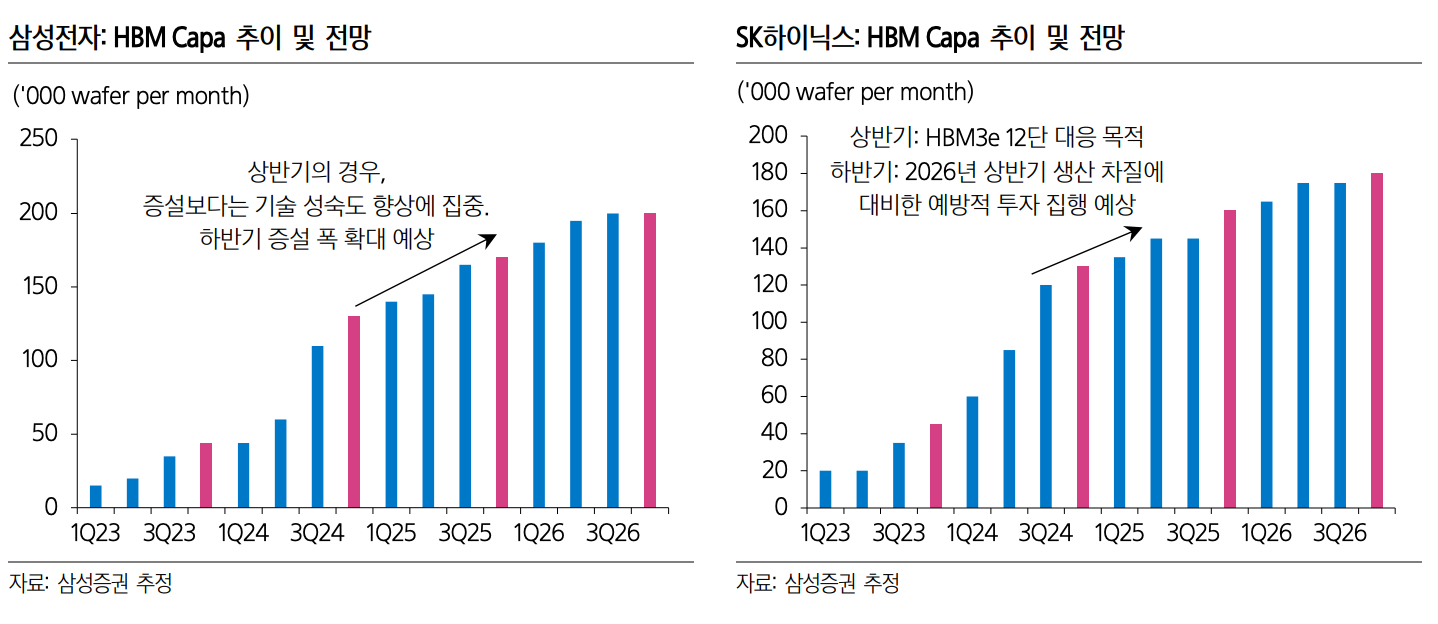
Micron Technology: Focusing on Achieving Targets Rather Than Excessive Investment
HBM capacity is expected to increase from 25–30K per month at the end of 2024 to 60–70K per month at the end of 2025. The goal for 2025 is to raise the HBM share to the level of the current DRAM share (in the early 20%s), and it is believed that this target could be achieved around Q3 2025. Since HBM and DDR5 are mass-produced using the DRAM 1b process—and given the constraints on front-end capacity—Capex is expected to be deployed in a pragmatic manner rather than pursuing an overly aggressive expansion of the HBM share.
Background of the Taiwanese Back-End Plant Acquisition
• The Hiroshima Plant Is at Full Capacity:
It is estimated that HBM front-end processing is currently being performed at Hiroshima Plant 1. The problem is that there is no available fab space. In the short term, a Taiwanese plant with available space must be used for HBM front-end processing, and in the medium to long term, Taiwanese and U.S. plants are expected to serve as forward bases for HBM front-end production.
To improve production efficiency, the back-end plant should be located close to the front-end facility. If the back-end plant is located too far away, wafers that have completed front-end processing would need to be transported by air to the back-end plant, thereby increasing logistics costs. Given the need to expand short-term production primarily through Taiwanese facilities, acquiring a back-end plant in Taiwan was deemed necessary.
• The TSV Process Requires Higher Cleanroom Specifications:
The TSV process demands higher cleanroom standards than those in existing back-end plants. The newly acquired plant was formerly used as an LCD factory, making it easier to configure an environment suitable for TSV processes (since display processes are similar to semiconductor processes). After remodeling to accommodate the TSV process, it is expected that the facility will be fully utilized for HBM back-end processing within the year.
Establishment of a New Singapore Back-End Plant: What Does It Imply?
A groundbreaking ceremony for the new Singapore back-end plant was recently held, and discussions regarding its utilization are active. It is anticipated that the plant will be used exclusively for advanced packaging. Moreover, it is highly likely that the facility was established with the versatility to be convertible for both HBM and NAND back-end processing.
• Singapore serves as Micron Technology’s forward base for NAND production, and it is estimated that there is some available land within the Singapore site.
• For next-generation NAND, it is expected that Hybrid Bonding will be applied to the cell-periphery structure, and it is believed that the new facility will partially implement the Hybrid Bonding process.

Direction of NAND Production in 2025
The Premise for Cycle Recovery Is Production Reduction
NAND Production Outlook for 2025
NAND production in 2025 is expected to grow by a modest 8% compared to the previous year. In NAND, the production increase effect from process conversion is greater than in DRAM—so much so that the industry is sometimes said to achieve a 15% production increase merely by “breathing.” Our forecast of an 8% production increase for 2025 assumes that some level of production reduction (i.e., reduced wafer input) will be implemented, and we believe that the effects of these cuts are likely to begin from Q2 2025. Currently, companies such as Kioxia, Micron Technology, and SK Hynix are discussing production restraint in NAND; although their approaches may differ, this trend is expected to spread throughout the entire NAND supply chain.
Why Reduce Production?
The primary reason is that the expectations for NAND demand have declined, and the competitive capacity expansion (the so-called “chicken game”) that characterized the past is no longer as effective. As a result, profitability is likely to become the top priority for businesses, and efforts to accelerate the cycle recovery through production control are expected to be further strengthened.
1. Declining Expectations for NAND Demand
• From 2015 to 2024, the annual average demand growth rate for NAND is estimated to have been around 30%. Demand experienced rapid growth due to factors such as the expansion of storage within IT devices (increased NAND adoption) and the substitution for HDDs (hard disk drives).
• However, recent NAND demand forecasts are not very optimistic. After 20 years of NAND’s existence, the high base created by previous growth makes further expansion more challenging, and in the short term, AI is not driving NAND demand growth to the same extent as it does for DRAM.
• Will Demand Remain Weak?
There are certainly triggers that could reverse the trend in NAND demand. High-capacity eSSDs, which are increasingly penetrating AI servers, could serve as a new growth driver. In 2024, Solidigm enjoyed a near-monopoly, but now several companies have reportedly completed quality testing for customer applications, and diversification of the supply chain tends to lead to the normalization of elevated prices. Consequently, from the customer’s perspective, there is a high likelihood of renewed adoption driven by the positive effects of eSSDs.
• For Now, Cut Production:
Although it is difficult to predict the exact timing, given the high volatility in demand forecasts, it appears more rational at this point to reduce industry inventories through production cuts rather than betting on uncertain demand. This approach is expected to help accelerate the cycle recovery.
2. The Reduced Effectiveness of the ‘Chicken Game’
• In past periods of weak demand, competitive capacity expansion—often referred to as a “chicken game”—would occur simultaneously. However, in today’s environment, the effectiveness of such a strategy is considerably lower.
• Semiconductors have now become strategic assets, and efforts to build domestic semiconductor supply chains are intensifying. Even if companies engage in a chicken game, no one is willing to let their domestic competitors fail. This new reality fundamentally reduces the effectiveness of capacity expansion competitions, making the normalization of supply through production cuts the top priority.
3. YMTC Is Unlikely to Have a Significant Short-Term Impact
• China’s NAND industry is led by YMTC, and YMTC—like CXMT—is expected to plan aggressive capacity expansion (forecasted to increase production by the mid-30% range year-over-year in 2025).
• However, capacity growth is expected to be limited. To mass-produce 3D NAND with 128 layers or more, support from global semiconductor equipment manufacturers is still required, but U.S. sanctions are anticipated to create challenges in securing such equipment.
• Although there is talk of replacing these with Chinese-made equipment—and companies such as Naura and AMEC are pursuing localization—it will take time before they achieve the technological level of industry leaders like Lam Research and Tokyo Electron.
• Given these limitations, YMTC is unlikely to have a dramatic impact on short-term NAND supply.
Evolution of DRAM Process Technology
The Era of 11nm (Feat. DRAM 1c)
Executive Summary
In the first half of 2025, DRAM 1c is expected to emerge. Starting with the pilot line and a small-scale mass production capacity setup in the first half, the full-scale expansion of DRAM 1c capacity is anticipated to begin in the second half. The market is expected to align with this trend by seeking out the technological changes and beneficiary stocks that will come to the fore with DRAM 1c.
What Will Be Emphasized?
The key technological change to be emphasized is the adoption of High‑K Metal Gate. While the applications in the DRAM 1a/1b segments have been largely limited to mobile and graphics, it is anticipated that these applications will further expand to include servers and PCs. This change aims to improve leakage current issues through the use of materials with high dielectric constants and to further enhance speed. As customer demand shifts toward high‑end products, the significance of this technology is expected to grow accordingly.
How Will Process Technology Change?
• EUV Layers: The number of EUV layers is expected to increase, which will help moderate the growth in etching process steps.
• Deposition Processes: There will be intensified efforts to deposit thinner and more uniform films. Changes are expected in the form of an increase in the number of ALD (Atomic Layer Deposition) steps and a higher proportion of Single‑Type systems within CVD (Chemical Vapor Deposition).
• Inspection/Measurement and Annealing: An increase in process steps for inspection, measurement, and annealing (using methods such as laser or high‑pressure annealing) is also anticipated. These changes are driven by the need to enhance yield improvement solutions.

DRAM 1c: How Will Process Technology Change?
1. Lithography Process: Expansion of EUV Layers
It is expected that EUV penetration within DRAM will increase. For instance, Micron Technology— which has not previously utilized EUV—plans to apply EUV for the first time in DRAM 1c and is believed to have already deployed EUV at its Hiroshima plant. Similarly, Samsung Electronics and SK Hynix are anticipated to increase their EUV layer counts. Through the expanded use of EUV, companies aim to control the growth in process steps that comes with further miniaturization and to seize opportunities for performance innovation.
2. Timing for the Introduction of High-NA EUV
High-NA EUV is not expected to be introduced until after DRAM 1c. For DRAM 1d, while pre-development is currently underway, the introduction of High-NA EUV remains uncertain. Although there is consideration for applying it to approximately one layer, the current outlook suggests that its adoption might be delayed until after DRAM 1d.
• To implement High-NA EUV, innovations in materials and components are essential. High-NA EUV operates with a higher source power compared to conventional Low-NA EUV, so changes in the materials/components to withstand the increased power are required before it can be applied in mass production.
• Even in DRAM 1c—which uses an increased number of Low-NA EUV layers—development has encountered challenges at the materials/components level. For example, in the case of photoresist, the industry has primarily relied on products from Infineon. Any issues have largely been due to the material composition; although these photoresists contain a high percentage of metal oxide with excellent selectivity, this component poses a limitation by potentially causing wafer contamination during non-metal processing.
• Given the significant changes that High-NA EUV is expected to bring, if the necessary innovations in materials and components do not occur, the industry will find it challenging to deploy High-NA EUV in DRAM 1d without hesitation. While there might be new equipment purchases for R&D purposes, breakthroughs in materials/components are critical for its broader adoption within DRAM.
2. Etching Process: Opportunity for ASP Growth Remains
• With the expansion of EUV layers, the growth in the number of etching process steps is expected to be limited. However, there remains room for growth in equipment ASP.
• The DRAM process follows a LELE (Lithography-Etching-Lithography-Etching) structure, essentially a repetition of sketching the circuit via lithography and then removing unwanted areas through etching.
• If the number of EUV layers increases within this structure, the overall increase in lithography process steps will be limited—since tasks that previously required multiple exposures with DUV can now be accomplished in one step using EUV—and the subsequent increase in etching process steps will also be constrained.
• Although the number of front-end process steps is rapidly increasing due to process miniaturization, the extent of the increase in etching steps may be limited by the expanded use of EUV layers.
• Nonetheless, there is still potential for additional growth in equipment ASP, as the need to etch in increasingly finer areas will drive continuous upgrades in equipment specifications.
3. Deposition Process
• Efforts to reduce film thickness for improved integration density will continue. The development direction in deposition technology is toward forming thinner and more uniform films.
• In pursuit of this, the number of ALD (Atomic Layer Deposition) steps—advantageous for thin film deposition—is expected to continue growing. While ALD was applied to fewer than five layers up to DRAM 1a, from DRAM 1c onward, its contribution could expand to 10 or more steps.
• In the CVD (Chemical Vapor Deposition) domain, which has an advantage in equipment throughput compared to ALD, the share of Single Type over Batch Type equipment is expected to increase. This is because processing each wafer uniformly using Single Type equipment can yield better film characteristics.
4. Other Processes
1. Process Control (Inspection/Measurement):
The difficulty of securing acceptable yields is increasing, and to enhance the effectiveness of yield improvement, the number of inspection/measurement steps is continuously expanding.
2. Annealing Process:
As a process that can help remedy yield-degrading factors (such as voids and interfacial defects) occurring during processing, additional annealing steps are expected. Techniques such as laser annealing and high-pressure annealing are anticipated to contribute.
Changes in AI Memory Semiconductor Process Technology: The Spread of Warmth and Diversification of the Product Portfolio
HBM4: Getting Stronger and Faster
1. Changes in Front-End Process Technology
HBM4 (6th generation) is expected to be launched in the second half of 2025, while HBM4e (7th generation) is projected to emerge between 2026 and 2027. Since HBM4 is scheduled to be partially supplied to major customers in Q4 2025, HBM4 pilot lines are expected to be set up between Q2 and Q3 2025. In the front-end process, major changes are anticipated in three key areas.
1. Efforts to Increase Bandwidth and the Rising Number of I/Os
For faster data processing, HBM4 is expected to further expand its bandwidth. It is anticipated that the number of I/Os—serving as the data transmission channels—will be doubled compared to HBM3e (from 1,024 I/Os in previous generation products to 2,048 I/Os in HBM4) to explore additional opportunities for bandwidth expansion.
• The background for GPU customers’ willingness to pay a premium for HBM ultimately lies in its superior bandwidth.
• In the conventional DRAM architecture, where the maximum number of I/Os was limited to 64, the data processing burden per pin was high, and in environments where large volumes of data are transmitted simultaneously, there exists a risk of errors. Reducing the data processing load per pin and maximizing data transfer speed fundamentally depends on increasing the number of I/Os.
Along with the increase in I/Os, chip size is also expected to grow relative to previous generations. However, given that the wafer size is limited to 12 inches, an increase in chip size will inevitably result in a reduction in net die (the number of chips that can be produced per wafer). Therefore, to minimize the decline in productivity, the growth in chip size must be properly controlled. To achieve this, technological development is expected to focus on creating a more refined TSV array.
How much will the Net Die decrease?
The reduction in Net Die count is expected to vary by supplier due to differences in the processes applied by each, but generally, it is estimated that the Net Die count will drop by approximately 20% compared to HBM3e. Consequently, as the HBM4 capacity share increases, the displacement effect of HBM on DRAM capacity is likely to further expand.
2) Mono Die Capacity Remains the Same as HBM3e
The Mono Die capacity of HBM4 is projected to remain at 24 Gb, identical to that of HBM3e. Although there were initial considerations to introduce a 32 Gb capacity to boost density, given the tight development schedule and rising technical challenges, the decision was made to maintain 24 Gb. The new 32 Gb capacity is expected to emerge starting with HBM4e.
3) Base Die: Adoption of New Logic/Foundry Processes
A notable development is the new integration of logic/foundry processes for the Base Die. Unlike in HBM3e—where both the Base Die and the Core Die were produced using DRAM processes—the Base Die in HBM4 will be manufactured using logic/foundry processes, and the mass-produced Base Die will then be bonded with the Core Die by the memory semiconductor companies. With the exception of Micron Technology, it is expected that all suppliers will adopt logic/foundry processes for the Base Die.
What will change?
Historically, the Base Die in HBM served as the controller, equipped with circuits that managed communication between Core DRAM dies and connected HBM to GPUs via PHY to enable high-speed data processing. As a result, the Base Die consumed a significant amount of power.
Currently, efforts are underway to mass-produce the Base Die using logic/foundry processes, and given its high power consumption, R&D is focusing on improving its power efficiency. Starting with HBM4, if changes in the Base Die materialize, its role is expected to expand further:
• Whereas HBM3e primarily functioned as a control unit, HBM4 is anticipated to directly perform some computational tasks.
• In addition to enhancing the conventional memory controller functions through logic/foundry processes, there is the added advantage of incorporating non-memory semiconductor IP to more precisely address customer requirements.
Can HBM4 Evolve into a Custom Semiconductor?
HBM4 is being developed along two main trajectories: one as a Standard HBM that conforms to JEDEC standards, and the other as a Custom version that incorporates additional customer requirements.
It is estimated that demand for Custom HBM is emerging—especially from major North American tech companies such as Nvidia and Broadcom—and the custom aspect of HBM is expected to be significantly reinforced starting with HBM4. Specifically, HBM4 is likely to be semi-custom, with a full-fledged entry into the Custom domain beginning with HBM4e.
• AI remains an unstandardized technology, with different companies pursuing varying directions in AI development and applying different technologies. As a result, customized features tailored to each company’s technological approach are likely to be emphasized.
• For HBM4, custom functions may be partially implemented by adding customer-requested IP in the interface area between the Base Die and the Core Die.
• The trend toward customization is expected to become more pronounced starting with HBM4e. While HBM4 incorporates IP developed within the HBM industry, beginning with HBM4e, customer IP can be integrated into the Base Die. Discussions are ongoing regarding approaches such as designing based on IP received from customers versus the HBM industry designing from the outset in line with customer requests. Ultimately, when Custom HBM produced through such collaborations is mass produced, it is anticipated that GPUs/NPUs will focus solely on AI computations, while additional operations—such as memory control—will be managed by the Base Die.


2. Changes in Back-End Process Technology
1. Bonding: Conventional Process Technology Will Be Maintained Through HBM4
HBM4 is expected to be offered in 12-stack and 16-stack configurations, and conventional technologies such as TC‑NCF and MR‑MUF are anticipated to continue being used through HBM4. With JEDEC’s height standard relaxed from 720 µm to 775 µm, the existing technology’s applicability is expected to be further extended. The market’s interest in Hybrid Bonding is high, but its penetration is forecast to be delayed until HBM4e.
Why Is the Adoption of Hybrid Bonding Delayed?
While Hybrid Bonding offers the technical advantage of enabling chip-to-chip bonding without bumps—thus allowing for a further reduction in the gap between chips—the relaxed JEDEC height standard now makes it possible to meet technical requirements without resorting to Hybrid Bonding.
Another challenge is the investment burden. The equipment required for Hybrid Bonding is inherently more expensive than standard back-end equipment, and it is estimated that converting 10K capacity to Hybrid Bonding would cost in the mid-to-high 100-billion range. Given the relaxed height standard, the benefit of paying a premium for new Hybrid Bonding technology is not substantial.
Additionally, the difficulty of implementing the technology remains an issue. The related ecosystem needs further development before the practical benefits of the Hybrid Bonding process can be fully realized. In the current environment—where even a 1% improvement in single-layer bonding yield is critical—there is little incentive to assume the risks associated with early adoption of Hybrid Bonding.
At What Stack Count Will Hybrid Bonding Be Applied?
It is believed that bonding can be successfully achieved without Hybrid Bonding up to 16 stacks. The penetration of Hybrid Bonding is expected to begin with 20-stack products, which are first introduced in HBM4e. Currently, various technical approaches are under discussion, and there is ongoing development of a hybrid method that employs both Hybrid Bonding and TC Bonding simultaneously.
• What Is the Hybrid Solution?
Assuming a total of 20 stacks, the configuration could be divided into 10 sets of 2 stacks each. Each two-stack set would be bonded using TC Bonding, and when joining one two-stack set with the next, Hybrid Bonding could be applied. This approach would reduce the gap between chips while simultaneously minimizing reliance on Hybrid Bonding.
2) The Wafer Becomes Even Thinner
For the mass production of high-stack products, the thickness of individual wafers or dies must be further reduced. In HBM3e, even though the package heights (cube heights) for 8-stack and 12-stack products are the same, thinning the wafer can significantly increase the difficulty of two key processes:
• Cutting Process:
As wafer thickness decreases, handling becomes more challenging. Whereas mechanical dicing was previously sufficient, the reduction in thickness may prompt new attempts to apply laser grooving. Discussions are reportedly underway regarding femtosecond laser grooving—which has throughput advantages for wafer processing—and major vendors are believed to be conducting quality tests on such equipment. Companies such as Disco and Iotechnique may play key roles in this area.
• Changes in Inspection/Measurement Technology:
A thinner wafer increases the risk of warpage (i.e., the bending of the wafer). As the number of stacking layers grows, the need for inspection/measurement equipment with higher detection capability increases, because insufficient detection power may lead to difficulties in identifying cracks. While Camtek’s equipment is currently in use, there is potential for the supply chain to expand with contributions from companies like NexTain and KLA.
New Memory: The Expanding Warmth of AI
1. The Emergence of SO-CAMM (Feat. GB300, PC, Server)
Nvidia’s GB300, expected to complete development by the end of the first half of 2025, is anticipated to introduce additional changes in the form factor of the integrated DRAM. Up to GB200, LPDDR5x standalone modules were used; however, for GB300, it is believed that a new form factor called SO-CAMM will be applied. This marks a shift from a standalone business model to a module-based structure, and as a new product, it is expected to offer excellent pricing and margins. In addition to HBM and high-capacity eSSDs, this opens up another opportunity for the memory semiconductor market to profit from AI.
What is SO-CAMM?
Compared to traditional SO-DIMM modules, SO-CAMM is expected to offer the following advantages:
• Contribution to Thickness Reduction:
By utilizing a small substrate, SO-CAMM can potentially reduce the module thickness by more than half relative to conventional SO-DIMM modules.
• Performance Improvement:
Allowing for shorter trace lengths compared to traditional SO-DIMM modules, SO-CAMM enables lower power consumption and higher operating speeds. It is seen as a new technology that can contribute to improvements in both data transfer speeds (i.e., bandwidth expansion) and capacity.
Based on these technical strengths, the total addressable market (TAM) is expected to continue expanding. Adoption attempts are emerging not only in AI GPUs but also in certain PCs, and it is anticipated that this product lineup will be continuously expandable into the server market.
Who Will Supply SO-CAMM to Nvidia?
Until GB200, Micron Technology is estimated to have exclusively supplied LPDDR5x standalone modules. With GB300, market share dynamics are expected to change, and both Samsung Electronics and SK Hynix are anticipated to address this demand using their DRAM 1b process.
2. Will There Also Be Changes for Mobile? (Feat. LLW/LPW)
In the future, the need for semiconductors with expanded bandwidth in mobile devices is expected to become more prominent. However, it is highly likely that this will not occur during the 2025–2026 period. At present, AI software is only beginning to penetrate mobile devices, and specialized semiconductors like HBM are expensive—driving up material costs. Given that AI software technology development is still underway, it is unlikely that system companies will attempt adventurous, high-risk initiatives in the near term. During 2025–2026, improvements in mobile AP performance and increases in memory semiconductor integration are expected to be the primary means of addressing the AI era.
However, from 2026 onward, new attempts to integrate semiconductors with increased bandwidth may emerge. As AI software performance and utility expand to the point where mobile devices can essentially serve as personal AI assistants, communication between devices and users—via text, voice, video, etc.—will diversify. To process this data without delay, ultimately, an expansion in bandwidth will be required. It is anticipated that the specifics of this requirement will become clearer around 2027.
• In hardware, to operate AI software, the data rate (transmission rate) will need to be increased several times over the current level.
• While increased capacity integration may be one response, the ultimate solution will likely be an expansion in bandwidth.
What Specifications Are Required?
For mobile integration, the semiconductor must be compact. Compared to PCs and servers, mobile devices face significant space constraints, making miniaturization crucial—a key reason why HBM has historically struggled to penetrate the smartphone market (despite its adoption in PCs, as seen with AMD, and in automotive applications, as with Waymo). Consequently, it is believed that technologies aimed at creating a compact product with a similar concept to HBM (i.e., increasing the number of I/Os) will prevail, and that these are currently being developed in the industry under names such as LLW/LPW. It is estimated that the number of I/Os has been successfully expanded to 512, and in the case of SK Hynix, there is a precedent where a similar type of semiconductor was supplied for Vision Pro applications.
• Historically, wire bonding (connecting copper wires) has been used to link DRAM and mobile APs. With the advent of the on-device AI era, the number of wires required is increasing, and space constraints are expected to become an issue. Additionally, increased DRAM integration may trigger new problems, such as an excessive increase in copper wiring length, which could in turn lead to reduced data transmission speeds.
• Samsung Electronics and SK Hynix are developing technologies such as VCS and VFO (Vertical Wire Bonding), respectively, and as AI software technology matures, it is anticipated that the integration of such new semiconductors will also gain traction.
Changes in NAND Process Technology: The Cell-Peri Structure Is Changing
Executive Summary
The stacking count of 3D NAND is advancing from the 200‑layer era toward the 400‑layer era, and along with this increase, new technologies are being introduced. A notable feature is that the Cell‑Peri structure is undergoing changes. It is anticipated that a new structure—where the Cell and the Peri are manufactured on separate wafers and then combined via Hybrid Bonding (Wafer‑to‑Wafer Bonding)—will establish itself.
First Change: Transformation of the Cell‑Peri Structure with Increased Penetration of Hybrid Bonding
Historically, the NAND industry has manufactured the Cell and the Peri on a single wafer using a structure that places the Peri below the Cell (known as COP: Cell Over Peri) to maximize the available area for the Cell.
• NAND Structure: NAND is composed of a Cell, which stores data, and the Peri, which comprises the peripheral circuits (in the CMOS area) that drive the Cell.
• Changes in the Cell‑Peri Structure:
• In 2D NAND, the Cell and the Peri were arranged side by side. With the transition to 3D NAND, to improve spatial efficiency, the structure evolved to place the Peri beneath the Cell.
• As the industry moves into the 400‑layer regime, it is expected that even the traditional COP structure will undergo modifications.
• It is anticipated that a new method—manufacturing the Cell and the Peri on separate wafers and then merging them using Hybrid Bonding (Wafer‑to‑Wafer Bonding)—will be adopted, opening up new investment opportunities amid these technological changes.
Second Change: Entering the Era of Triple Stacking
With Samsung’s V9 platform (estimated at 286 layers) serving as a turning point, the era of double stacking is drawing to a close.
• Now, the era of triple stacking has arrived, and it is expected that the stacking count of NAND will leap from over 300 layers into the 400‑layer range.
• Key Considerations:
• To rapidly increase the stacking count in 3D NAND, it is crucial to maximize the number of Gates that can be implemented in a Single Stack. In order to increase the number of layers that can simultaneously form a Channel Hole, the thickness of the films constituting NAND must be minimized.
• Whereas the achievable layer count in a Single Stack was previously around 130–140 layers (based on the number of Gates), current trends indicate that this can now be raised to approximately 150–160 layers. In Samsung’s case, it is believed that they have already secured technology capable of handling up to 160 layers in a Single Stack.
Customer-Specific Tech Roadmap: 3D NAND in the 400‑Layer Era in 2025
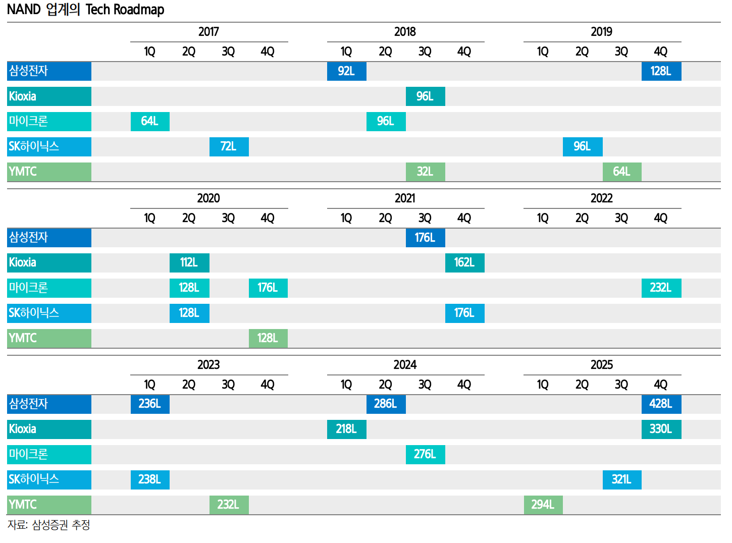
1. Samsung Electronics: Going Straight to 400 Layers in 2025
1. 2024:
• In April 2024, Samsung Electronics launched a new platform, V9 (estimated at 286 layers with double stacking), and became the first in the industry to begin mass production of 1 Tb TLC products.
• They reduced the cell area by eliminating Dummy Channel Holes (channel holes created in the cell array to distinguish between planes, which do not function in operation) and improved product quality by applying cell interference avoidance and lifespan extension technologies to mitigate interference issues caused by reduced cell sizes.
2. 2025:
• It is projected that by Q4 2025, Samsung will complete development of V10 (estimated at 428 layers, utilizing triple stacking).
• With current technology supporting up to 160 layers in a Single Stack, the application of triple stacking is expected to propel the stacking count from over 300 layers directly into the 400‑layer range.
• A key structural change will be in the Cell‑Peri configuration, with a shift from the COP (Cell Over Peri) structure to one that utilizes Hybrid Bonding (Wafer‑to‑Wafer Bonding).
2. SK Hynix
1. 2024:
• SK Hynix has completed development of a 321‑layer structure (using triple stacking). Although the new platform development is complete, due to NAND production restraint, mass production volumes for the 321‑layer product have not yet been realized.
2. 2025:
• It is expected that mass production of the 321‑layer product will commence partially in the second half of 2025, driven by the need to respond to the expanding demand for high‑capacity eSSD (QLC products) in on‑premise servers.
• Following the 321‑layer platform, the next generation is expected to reach the 480‑layer range, and from that point onward, the adoption of Hybrid Bonding (Wafer‑to‑Wafer Bonding) is anticipated to be implemented on a full scale.
3. Kioxia-Western Digital
• At the end of March 2023, Kioxia-Western Digital launched a 218‑layer 3D NAND (BiCS 8) and became the second company, after YMTC, to apply Hybrid Bonding (Wafer‑to‑Wafer Bonding) to a Cell‑Peri structure.
• It is expected that they will subsequently launch a 128‑layer product (with improved I/O speeds through Single Stack technology) and a 330‑layer high‑stack product.
4. Micron Technology
• Micron is currently mass-producing products based on 176‑layer and 232‑layer structures.
• It is expected that, in the first half of 2025, Micron will begin releasing products in the 300‑layer range employing triple stacking.
5. YMTC
• YMTC began applying Hybrid Bonding (Xtacking) starting with its 64‑layer 3D NAND, and it is estimated that they are now exploring a new platform approach (Xtacking 4) that involves stacking three wafers.
• Additional Considerations for YMTC:
• They are reportedly encountering technical difficulties in Channel Hole Etching due to U.S. sanctions.
• YMTC is considering applying a new technology called Xtacking 4 to expand the stacking count. This method involves stacking two Cell Array wafers onto a logic wafer (i.e., stacking three wafers in total), which could be advantageous for increasing the stacking count; however, precise alignment during the stacking process is critical, making yield assurance extremely challenging.
• It is estimated that they have recently succeeded in developing a new 294‑layer platform based on this technology, but due to the exceptionally high technical difficulty, achieving acceptable mass production yields remains a significant challenge.
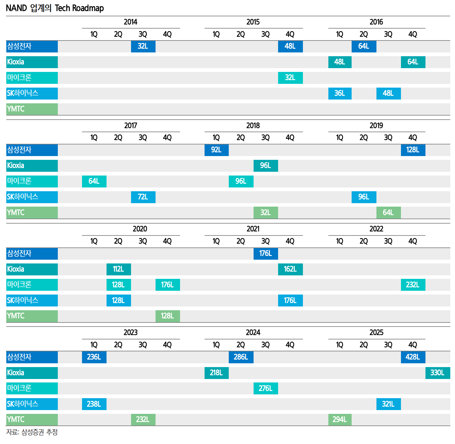
Penetration of Hybrid Bonding Is Gaining Momentum
What technology has been applied so far?
Except for YMTC, the NAND industry has been developing technology by using a structure that places the Peri (peripheral circuitry) beneath the Cell in the unusual 92/96-layer designs. Examples include Samsung’s COP (Cell Over Peri), SK Hynix’s PUC (Peri Under Cell), Micron’s CUA (CMOS Under Array), and Kioxia’s CMOS Bonded Array. Only YMTC has been developing technology using Xtacking, starting from 64 layers.
What are the benefits of placing the Peri beneath the Cell?
• In 2D NAND, the Peri (logic area) was arranged on the same plane next to the Cell.
• By positioning the Peri underneath the Cell, the chip size can be reduced while increasing the effective area available for the Cell, thereby improving overall quality.
• Typically, the Peri occupies about 20–30% of the total area; placing it under the Cell enhances design efficiency. Leveraging these technical advantages, SK Hynix has applied this structure from 96 layers onward, while Samsung, Micron, and Kioxia have done so from 176 layers onward.
What advantages will the introduction of Hybrid Bonding as a new technology bring?
Background for Adopting Hybrid Bonding:
As process technology advances (with increasing stacking counts), the technical difficulty of implementing the traditional COP (Cell Over Peri) structure has begun to rise. With taller Cells, forming interconnects becomes more challenging, and issues such as quality degradation due to thermal processes have started to emerge.
• In 3D NAND using the COP structure, the Peri is typically manufactured first, followed by the basic formation of the Cell—similar to a mixed-use building where shops occupy the lower floors and residences the upper floors.
• After the Peri process, the Cell is added. In this step, high-temperature processes are sometimes employed, and the Peri region can suffer performance degradation due to increased thermal stress.
Improved Operational Speed:
Hybrid Bonding does not solely offer advantages over the COP structure. Unlike COP—which integrates both Peri and Cell on a single wafer—Hybrid Bonding uses two separate wafers, making its adoption in the cost-sensitive memory industry challenging; in fact, YMTC, which has newly applied Hybrid Bonding, has experienced abnormal losses.
Nevertheless, despite its cost disadvantages, the expansion of Hybrid Bonding is driven by its performance benefits—particularly significant improvements in operating speed.
• With Hybrid Bonding (Wafer-to-Wafer Bonding), the Cell and Peri are manufactured on separate wafers and then bonded together, which is inherently more expensive than placing both on a single wafer (as in the COP structure).
• However, this method reduces the thermal stress imposed on the Peri region during processing and can shorten both development and mass production lead times.
• Most importantly, the undeniable benefit is the enhancement in operational speed. Considering that operating speed is a key indicator of quality improvement demanded in major applications such as servers and mobile devices, the industry’s adoption of Hybrid Bonding is expected to continue growing.
Who Will Use It and When?
Starting with Samsung Electronics’ new adoption in 2025, it is expected that roughly half of the NAND industry (Samsung Electronics, Kioxia, and YMTC) will implement Hybrid Bonding.
• Samsung Electronics: Hybrid Bonding is anticipated to be applied starting with the V10 platform—estimated at 428 layers with Triple Stacking—which is expected to be completed around Q4 2025.
• SK Hynix: The existing PUC (Peri Under Cell) structure is expected to be maintained up to 321 layers; however, from the next-generation platform of 480 layers onward, new adoption of Hybrid Bonding is anticipated.
• Kioxia and YMTC: Both have already implemented Hybrid Bonding in their launched platforms (Kioxia began applying it from 218 layers, while YMTC has been using it since 64 layers) and are expected to continue expanding its application across additional technology nodes.
What Hybrid Bonding Technology Is Applied in NAND?
Hybrid Bonding is a technology derived from the mechanism of joining two objects without an adhesive (paste material). By directly bonding the pads of copper wiring—without using bumps that traditionally serve as an adhesive—this method shortens interconnection lengths, reduces power consumption, and significantly improves electrical signal density. In NAND, the adoption of a Wafer-to-Wafer Bonding structure is expected.
1. Wafer-to-Wafer Bonding
• As the term implies, this method bonds entire wafers directly to one another.
• It has been used, for example, when stacking DRAM on a CMOS Image Sensor, and its application is expanding toward next-generation 3D NAND.
• One limitation of this technology has been the difficulty in securing high yield—it can only bond objects of the same size, and stacking multiple layers has historically been challenging.
• To address these limitations, another form of Hybrid Bonding, known as Die-to-Wafer Bonding, has been developed.
2. Die-to-Wafer Bonding
• This approach is gaining attention in the market, particularly in 2.5D Packaging (e.g., TSMC’s CoWoS, Samsung’s I-Cube, Intel’s EMIB).
• Its advantage lies in the ability to selectively use only “good” dies (i.e., high-quality ones).
• Although it is currently predominantly used in 2.5D Packaging, its application is expected to expand to HBM (with anticipated application in HBM4e).
Who Will Benefit?
1. Pre-Processing: The Growing Importance of the CMP Process
• Finer Pitch:
For Hybrid Bonding (Wafer-to-Wafer), which is expected to gain increased penetration in NAND, there is historical precedent from its use in CIS. At that time, the required pitch was on the order of several micrometers. In NAND, however, this specification is anticipated to be tightened—estimated to require a pitch below 1 µm—thereby increasing the process difficulty.
• Enhanced Surface Management:
Because wafers must be bonded to one another, more precise surface management will be essential. Control of warpage, particle contamination, and dishing must be further enhanced.
• It is expected that micro bumps will be used, and the height of each bump must be kept more uniform. Variations in bump height could lead to poor connections—some areas might experience excessively tight bonding (hard contact), while others might bond too loosely (soft contact).
• Particle control is also critical. Even the presence of a 1 µm particle can interfere with dielectric bonding. If the bonding process fails to control particles under pressure, they may harden into “hard particles” that cause cracks; during thermal processes, even small particles might expand by over 100 times.
• Key Areas of Importance:
CMP (a process that planarizes surfaces, similar to sanding) and inspection/measurement will become increasingly crucial.
• CMP Process:
This is the core process for surface control, and the introduction of Hybrid Bonding is likely to lead to additional CMP steps.
• Inspection/Measurement Process:
Ensuring that pads are properly bonded will require equipment beyond conventional optical systems. Optical techniques may only detect voids caused by particles at the interface, so advanced, high-resolution measurement solutions (such as those based on atomic microscopy) are expected to emerge.
2. Supply Chain Considerations
• CMP Process Equipment:
CMP equipment is expected to be supplied primarily by companies like Applied Materials and Ebara. In terms of materials, domestic companies may also contribute; for example, Solbrain, Dongjin Semichem, and KCTech could play significant roles.
• Inspection/Measurement Equipment:
As fine measurement becomes essential for particle control, companies with advanced measurement solutions—such as Park Systems—may find significant new opportunities.
3. Bonding and Annealing Processes
• Bonding Process:
Accuracy, bonding strength, and speed will be the key capabilities. Companies such as EVG and BE Semiconductor are expected to contribute significantly in this area.
• Annealing Process:
Both low-temperature and high-temperature annealing will be necessary, and high-pressure technology may be utilized.
• Low-Temperature Annealing:
This involves annealing at around 150°C to form shared bonds.
• High-Temperature Annealing:
Raising the process temperature from 150°C to 350°C allows copper to expand, filling gaps caused by dishing, and transforming the structure so that the top and bottom surfaces come into contact.
• In the Cell region, high-pressure high-temperature annealing may be used, while in the Peri region, high-pressure annealing is likely to be employed.
thank you