


Hyundai Motor Securities – Field Trip Report on Japanese and Taiwanese Companies (HBM Market Outlook, Latest on SMIC, and Progress of HBM Localization in China)
This post is an English translation of a report by Hyundai Motor Securities.

TLDR: IT H/W
Review of Visits to Japanese and Taiwanese Companies
Field Trip Conclusions
① Expansion of the AI Semiconductor Ecosystem in the U.S., Japan, and China / Vertical Surge in HBM Demand in the Second Halves of ’25 and ’27
• Through visits to Taiwanese and Japanese companies, we have observed that in the U.S. and Japan, AI semiconductor demand is being driven not only by existing CSPs but also by new project demand momentum—for example, from projects such as Stargate and Cristal. In China, various efforts are underway to localize HBM production alongside AI semiconductor initiatives.
• In particular, it was confirmed that in the U.S., TSMC is planning to build six semiconductor fabrication plants, two back-end process plants, and one R&D center with a total investment of USD 165 billion. Additionally, TSMC is constructing five new 2nm fabs in Kaohsiung in addition to its existing facility in Hsinchu.
• When all the factories currently under construction are fully operational, it is expected that the share of cutting-edge fabs (5nm and below) will be approximately 60% in Taiwan and 40% in the U.S.
• Meanwhile, the Stargate Project is slated to invest USD 500 billion over four years to build AI data centers, with more than 90% of the required funds expected to be raised through project financing. GPU demand related to the Stargate Project is projected to reach approximately 400,000 units this year, and Oracle’s market share in the North American CSP market is anticipated to rise.
• In Japan, three AI data centers are planned to be built to support the enterprise Cristal service, a joint venture between SoftBank and Open AI.
• In China, competition in the commodity memory market is expected to intensify as not only CMXT but also YMTC are anticipated to enter the DRAM market.
• According to NVIDIA’s GPU Roadmap, the second halves of 2025 and 2027 are expected to witness a quantum jump in HBM content, reinforcing the strategic emphasis on the HBM segment.
② The AI Memory Megatrend Persists, and Capacity Expansion among HBM Makers is Intensifying
• There have been recent concerns regarding the surge in AI GPU demand and the expansion of HBM capacity. However, our analysis indicates that the leading HBM provider is currently struggling to fulfill all customer orders due to excess demand, prompting an accelerated capacity expansion compared to last year.
• Several indicators confirm this situation:
1. The order volume for Advantest T583x has been significantly revised upward compared to the end-of-last-year plan.
2. Additional orders are expected from domestic Burn-In tester providers.
3. There have been requests for capacity expansion from domestic Burn-In tester providers.
4. Bonder order volumes have also been recently revised upward relative to last-year-end plans.
5. Some legacy factories are being converted into HBM production facilities (scheduled for completion this year and next year).
6. Legacy equipment is being removed from joint legacy/HBM production plants and replaced with HBM-specific equipment.
• It is anticipated that, as HBM makers aggressively expand capacity, the growth of both new and existing HBM equipment vendors will become increasingly pronounced.
③ Electronics/Display: A Bottom-Up Approach Within the Sector is Effective This Year
• Contrary to the rapid growth in AI, IT demand remains shrouded in uncertainty. Despite the initially optimistic expectations from Chinese subsidy effects, unfavorable macroeconomic conditions and tariffs continue to weigh on IT demand. IT demand is expected to remain at a low- to mid-single-digit percentage level this year, suggesting that the electronics/electrical industry will continue to face a challenging environment.
• In the display sector, despite the contraction in IT demand, the industry is expected to benefit from strengthened positioning in OLED and cost improvements, thereby continuing to enjoy the effects of previous investments.
Top Picks: SK Hynix, Techwing, Samsung Electro-Mechanics, and Duksan Neolux
• Semiconductor Sector: SK Hynix is the top pick, as it is expected to benefit from the growth in the HBM market.
• Semiconductor Materials & Equipment: Techwing is recommended as the top pick, with growth anticipated from Cube Prober.
• Electronics/Electrical Sector: Samsung Electro-Mechanics is proposed as the top pick due to improved profitability from increased MLCCs for IT, automotive, and server applications, as well as the prospect of new business momentum.
• Display Sector: Duksan Neolux is highlighted as the top pick, driven by anticipated earnings growth from expanded Green Prime sales due to M14 expansion, along with momentum from Black PDL, foldable displays, IT OLED, and an increased proportion of sales to China.
• Overseas Interest: Advantest and IBIDEN are also noted as companies of interest.
Asian Corporate Field Trip Overview
Conclusion of the Visit to Taiwanese/Japanese Semiconductor Companies: Expanded Investment to Secure AI Leadership
① Memory Semiconductor and Foundry Sectors
From March 24th to 27th, we visited key semiconductor, display, and consumer electronics companies in Japan and Taiwan. During the trip, we assessed these companies’ H1 performance forecasts and their views on the industry.
First, TSMC, under pressure from U.S. government tariff measures, plans to invest in the U.S. by constructing three new semiconductor fabs, two back-end processing plants, and one R&D center—in addition to its existing three fabs in Phoenix, Arizona. In Taiwan, TSMC is also planning to build a total of six 2nm fabs, and it is expected that the share of advanced fabs (5nm and below) will be approximately 60% in Taiwan and 40% in the U.S. going forward. Although U.S. tariff pressures are a major factor driving TSMC’s large-scale U.S. investments, power supply shortages in Taiwan resulting from the nuclear phase-out have also played a role.
Meanwhile, through meetings with Japan’s SoftBank, we confirmed that the company is committing all its resources to advancing AI competitiveness in both the U.S. and Japan. In particular, aside from the Stargate Project with OpenAI and Oracle, the Japanese government is expected to actively support Cristal—a corporate AI service in partnership with OpenAI.
On another note, information from the Taiwanese supply chain indicates that China’s semiconductor drive is planning to expand into the commodity DRAM market with YMCT and intends to commence mass production of LPDDR5 products by 2027. Additionally, CXMT is already mass producing LPDDR5 using a 15nm process and is preparing to begin mass production of HBM3e in 2027. SMIC, Huawei, Sicarrier, and others have successfully achieved 5nm mass production using DUV, with these products expected to be deployed starting with Huawei’s Ascend 910C. Notably, these products incorporate HBM2e, confirming that China is also investing considerable efforts in domestic HBM production.
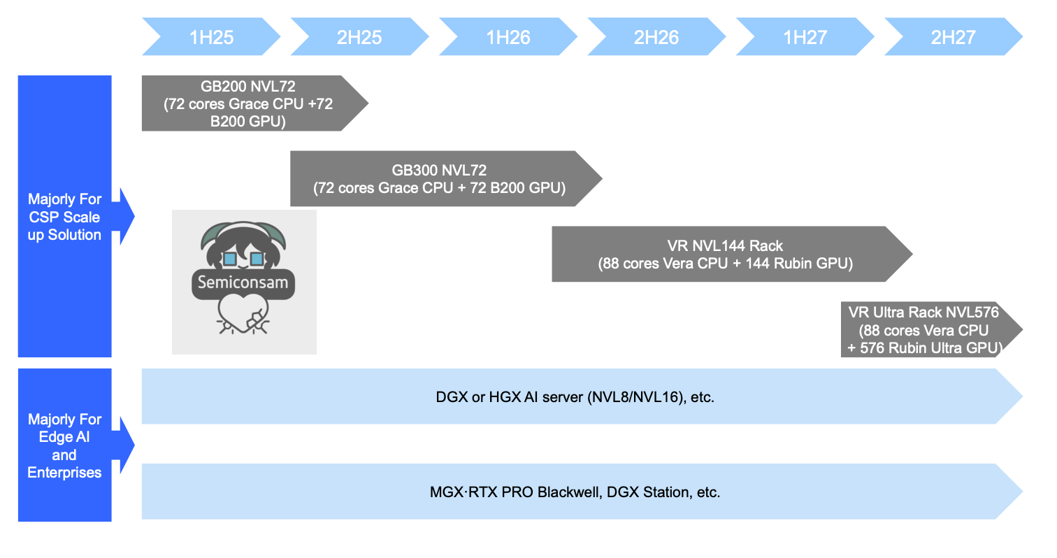
At the GPU Technology Conference (GTC) 2025 held in March, NVIDIA unveiled its roadmap for next-generation AI semiconductors. In particular, Blackwell GPUs achieved sales of 3.6 million units to the four major CSPs in North America—an increase of 176.9% year-over-year compared to the 1.3 million Hopper GPUs sold in 2024. Furthermore, NVIDIA revealed detailed specifications for several upcoming products: in the second half of this year, the Grace Blackwell Ultra NVL72 will feature 288GB of HBM content; in the second half of 2026, the Vera Rubin NVL 144, which combines the Vera CPU and Rubin GPU (with 144 GPUs); and in the second half of 2027, the Rubin Ultra will be equipped with 1TB of HBM. Most importantly, despite various uncertainties, it is expected that the DRAM market will also experience a quantum leap, given that HBM content is anticipated to take a quantum jump in the second halves of 2025 and 2027.
Meanwhile, since the end of March, there have been early signs of a rebound in commodity memory semiconductor prices, with memory semiconductor companies actively requesting price increases from their customers. Recent stabilization in commodity memory prices is being driven not only by factors such as customer inventory clearance, U.S. semiconductor tariffs, and stockpiling in anticipation of additional sanctions, but also by the reallocation of commodity memory wafers to HBM production. In some cases, as certain companies convert NAND capacity to HBM, the natural decline in NAND production is expected to continue into the second half of the year.
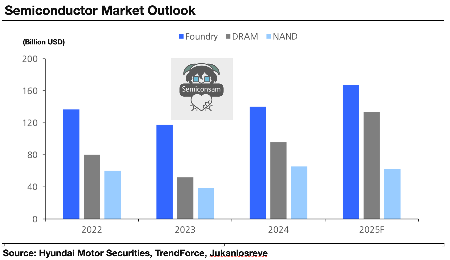
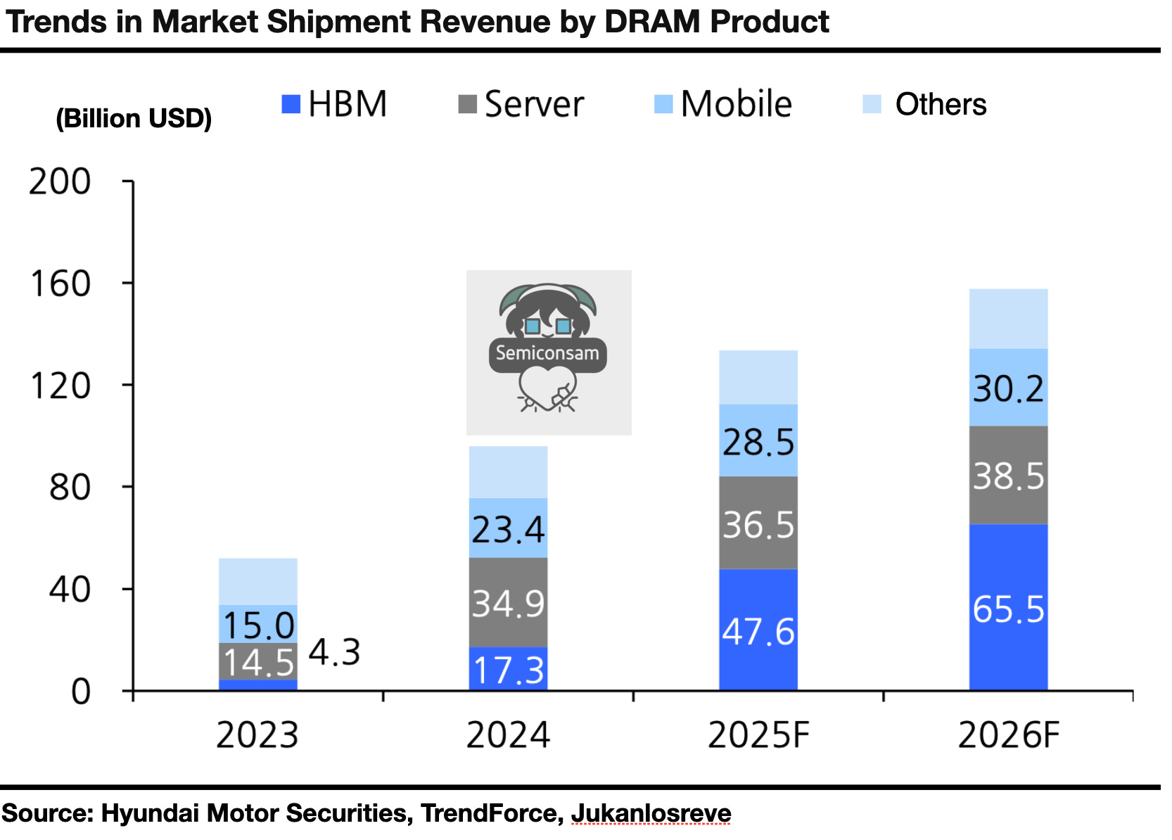
The share of HBM in DRAM is expected to account for 10% by shipment volume and 36% by value this year, and is projected to rise to 41% by value in 2026. Reflecting stronger-than-expected HBM demand and its positive spillover effect, the DRAM market size for this year has been revised upward by 22.4% to USD 133.5 billion. The overall memory semiconductor market is anticipated to reach USD 195.8 billion this year, marking a 21.2% year-over-year increase. Meanwhile, the global foundry market is expected to record USD 167.1 billion this year, a 19.4% YoY increase, driven by the growing demand for AI semiconductors. Additionally, TSMC, which virtually monopolizes the global HPC AI semiconductor market, is forecast to achieve consolidated revenue of USD 113.8 billion—a 26.4% year-over-year increase—with its market share rising from 64.4% in 2024 to 68.1%.
Conclusion from Visits to Taiwanese/Japanese Semiconductor Back-End Companies: The AI Memory Megatrend Persists and HBM Makers Are Rapidly Expanding Capacity
② AI Semiconductor and HBM Sector
During this business trip, we once again confirmed that the AI semiconductor megatrend—including both AI GPUs and HBM—remains extremely robust. Although there are concerns regarding AI GPU demand due to some big tech companies delaying investments and the emergence of a lighter model, DeepSeek, in the Greater China region, TSMC’s CoWoS capacity reservations have actually increased further in March compared to the beginning of the year—with NVIDIA up by 10% (from 400K to 437K) and Broadcom up by 10% (from 68K to 75K).
Furthermore, our visit to Japan’s Advantest confirmed that HBM makers are accelerating their capacity expansion. Advantest broke its historical quarterly record, driven by a significant surge in orders for its HBM Tester T583x, and even second-tier vendors, such as domestic HBM tester companies, have been receiving order volumes exceeding expectations.
In addition, the current leading HBM provider is expanding capacity through every available means to address the continuously growing customer demand. These measures include:
1. Requesting capacity expansion from domestic Burn-In tester providers;
2. Recently revising upward the order volume for bonders compared to the end-of-last-year plan;
3. Converting some legacy factories into HBM production facilities (scheduled to be completed this year and next year); and
4. Withdrawing legacy equipment from joint legacy/HBM production plants and replacing it with HBM-specific equipment.
This comprehensive capacity expansion is expected to yield significant benefits for HBM equipment vendors, and meaningful performance growth is anticipated for both new and existing HBM vendors this year.
Conclusion from Visits to Taiwanese/Japanese Electronics/Display Companies: A Bottom-Up Approach Within the Sector is Effective This Year
③ Electronics/Display Sector
It is evident that demand for smartphones, PCs, and conventional servers—excluding AI servers—remains weak. Expectations for an IT demand recovery driven by factors such as Chinese subsidies are unlikely to reverse this trend. Smartphone demand is expected to continue its sluggish performance, and the impact of Chinese subsidies is not anticipated to be significant in the short term. However, if inventory clearance in China occurs faster than expected, companies with a significant exposure to the Chinese market may experience additional upside in their performance.
Apple’s iPhone, despite the optimistic outlook fueled by the introduction of AI features this year, is still facing downward pressure from weak Chinese demand. Although smartphone sales from Chinese OEMs have increased due to Chinese IT subsidies, iPhone demand remains stagnant. The effect of the upcoming iPhone 16e launch is also expected to be modest. While there is potential to drive replacement demand for legacy models, the relatively high price compared to existing mass-market models is likely to result in weaker-than-anticipated sales. Moreover, considering that tariffs could further dampen demand, optimistic expectations for Apple appear unwarranted. We may have to wait for events like WWDC to see further developments.
Nevertheless, in this environment the domestic display industry is expected to maintain a profit growth trend compared to last year and potentially outperform within the IT sector. From a top-down perspective, positive factors include the partial securing of Chinese volumes due to the transition to TFT in iPhones and favorable exchange rates. In such an environment, it is particularly important to focus on companies that can achieve growth from a bottom-up perspective.
As previously noted, demand for smartphones, PCs, and conventional servers—excluding AI servers—remains weak, and the recovery in IT demand driven by Chinese subsidies is unlikely to reverse this trend. Smartphone demand is expected to remain subdued, though if Chinese inventory clearance occurs faster than anticipated, stocks with significant exposure to the Chinese market could see additional upside.
④ Industry Outlook and Top Picks
We maintain a positive outlook on the semiconductor sector, which is expected to benefit from increased HBM demand driven by expanded investments in AI data centers. Our top pick in the Korean semiconductor sector is SK Hynix, which is anticipated to further strengthen its dominance in the HBM market. For small- and mid-cap stocks, we recommend Techwing, which is expected to grow due to its Cube Prober.
Additionally, despite the prevailing uncertainty in IT demand, Samsung Electro-Mechanics is our top pick within the electronics/electrical sector, as increased MLCC demand for automotive and server applications is expected to improve profitability, with new business momentum on the horizon. In the display sector, Duksan Neolux stands out as our top pick, as it is expected to achieve substantial profit growth in the second half of the year driven by expanded Green Prime sales resulting from the M14 expansion, coupled with momentum from Black PDL, foldable displays, IT OLED, and an increasing share of sales to China.
AI and Memory Semiconductor Industry
Amid the Rising Demand for NVIDIA Blackwell and Custom Accelerators, Strong HBM Demand Is Expected to Continue
At NVIDIA’s GTC (GPU Technology Conference) 2025 held in March, CEO Jensen Huang emphasized that 3.6 million Blackwell products have been sold to the top four CSPs in North America (including reserved orders). This figure encompasses dual rack products such as the GB200 NVL72, module products like the GB200, and standalone Blackwell units—but it is estimated not to include Blackwell Ultra (B300), which will be supplied in the second half of the year.
When this figure is converted to bits, it totals 5,530 million Gb, representing approximately 30.7% of the total HBM demand for this year. Considering the upcoming release of the B300 in the second half, as well as existing products such as the H200, H20, and other Blackwell orders for specific clients, it is anticipated that NVIDIA will account for over 70% of the overall HBM demand.
Meanwhile, NVIDIA sold 1.3 million Hopper GPUs to the top four CSPs in North America last year.
At the recent GTC, NVIDIA unveiled the detailed specifications for its Vera Rubin and Rubin Ultra products. The Vera platform supports 88 custom ARM cores, 176 threads, and an NVLink-C2C bandwidth of 1.8 TB/s. The Rubin platform is equipped with 50PF FP4 and 288 HBM4, while the Rubin Ultra will feature a GPU with 4 dies, 1000PF FP4, and 1 TB of HBM4e. Ultimately, the quantum leap in HBM content will be delivered by Black Ultra (288 GB) and Rubin Ultra (1 TB), with the first phase of this quantum jump expected in the second half of this year. Of course, whether demand will respond in line with NVIDIA’s long-term roadmap by 2027 remains uncertain, as North American CSPs continue to adjust their investment pace in AI data centers and, following DeepSeek, there is a growing focus on rationalizing capex. Nonetheless, with increasing demand for various forms of agentic AI, physical AI, and edge AI, the advancement of AI semiconductors for training purposes remains essential. NVIDIA is expected to persist in providing best practices for building power-efficient data center infrastructure through its differentiated custom CPU, NVILink technology, and GPU design expertise. Additionally, rising demand among not only North American CSPs but also among 2nd-tier CSPs, enterprises, telecom operators, and sovereign AI initiatives suggests that overall AI semiconductor demand will trend upward.
Meanwhile, as HBM demand surpasses expectations, major DRAM manufacturers are increasing the HBM allocation per DRAM wafer. Some companies are even converting NAND capacity to HBM, accelerating the natural reduction of commodity DRAM and NAND production. Consequently, early signs indicate that prices for commodity DDR5 and NAND products are rebounding—reflecting a positive spillover effect from HBM across the entire memory industry. However, given that Chinese companies like CXMT, which mass-produce low-cost DRAM, continue to accelerate their market penetration, the trend toward long-term stabilization of commodity product prices appears unlikely. That said, with HBM demand emerging even stronger than anticipated, annual DRAM and NAND demand for this year is expected to exceed market forecasts. It is projected that HBM will account for 10% of DRAM shipments by volume and 36% by value this year, with the value share rising to 41% by 2026.
Reflecting better-than-expected HBM demand and its positive spillover effect, this year’s DRAM market size has been revised upward by 22.4% to USD 133.5 billion. The overall memory semiconductor market is projected to reach USD 195.8 billion this year, representing a 21.2% year-over-year increase.


Analysis of the Impact of U.S. AI Semiconductor Demand and Tariff Impositions
Since February of this year, there have been rumors that the U.S. government has requested TSMC—the world’s leading foundry—to either provide technical assistance to Intel or to acquire Intel. In fact, foreign media have reported that if TSMC does not comply, the U.S. government may either initiate an antitrust review of TSMC or impose high tariffs on it. However, we have pointed out that if TSMC were to acquire Intel’s manufacturing division, it would fall under antitrust scrutiny, and given the low likelihood of such a transaction being approved in regions like China and Europe, this scenario is unlikely to materialize.
Since 2023, Intel has restructured its business model by segregating its operations into manufacturing and design divisions—moving away from its previous structure, where only external customer revenues were reflected in its foundry revenues. Under this new structure, Intel Foundry—the manufacturing division—has recorded quarterly revenues of USD 4.3–4.5 billion, with operating margins ranging from –50.2% to –134.3%. However, when Intel Foundry’s revenue is defined on an Intel basis, it surpasses that of Samsung Electronics’ foundry business, suggesting a scenario where the leading company could potentially acquire the second-ranked firm.
Meanwhile, in response to the U.S. government’s demands, TSMC has announced plans to invest USD 100 billion in the United States, which includes the construction of three semiconductor fabrication plants, two back-end processing facilities, and one R&D center. With the addition of this new investment to its existing USD 65 billion, TSMC’s total investment is projected to reach USD 165 billion. In particular, as TSMC is even building back-end processing facilities, it is expected that its supply chain partners—such as ASE—will also construct a significant number of new plants in the United States.
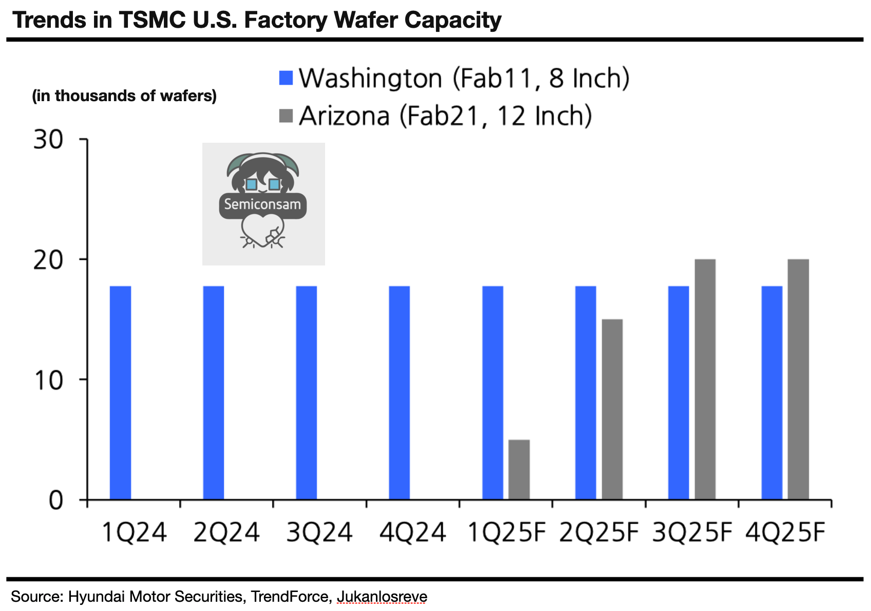
TSMC has three fabs in Phoenix and has announced investments of USD 12 billion for Fab21 Phase 1, USD 28 billion for Phase 2, and USD 25 billion for Phase 3, with a confirmed subsidy of USD 6.6 billion from the U.S. government. Fab21 Phase 1, which utilizes a 4nm process, is set to begin operations at the end of 2024; Fab2 will employ a 3nm process and is expected to start in 2028; and Fab3, which will use a cutting-edge process at 2nm or below, is planned to commence around 2030. The three fabs announced this time (Phases 4, 5, and 6) are ultimately expected to enable mass production of products at the 1.6nm and 1.4nm nodes.
If TSMC also builds back-end processing facilities, such as CoWoS fabs, in the United States, the tariff risks on AI semiconductors consumed domestically are expected to be completely mitigated. Currently, Taiwanese companies with server assembly lines in the U.S. include Foxconn (in Texas and Wisconsin), Qunata (in California and Tennessee), and Wistron (in California), and additional new plant constructions by Taiwanese ODMs in the U.S. are anticipated. In the back-end sector, Amkor is expanding its facility in Phoenix, and until the new CoWoS fab is completed, utilizing Intel’s back-end facilities might also be considered.
Moreover, for recent logic semiconductor products characterized by a chiplet architecture, if TSMC handles the advanced 4nm/3nm processes while mature processes (10nm and above) are managed by Intel, this division of responsibilities could significantly improve the utilization rates of Intel’s fabs. Currently, Intel operates fabs in the United States located in Oregon (The Silicon Forest, operational since 1974), Arizona (The Silicon Desert, operational since 1979), and New Mexico (The Silicon Mesa, operational since 1980), and it broke ground on a new fab in Ohio (The Silicon Heartland) in 2022.
Meanwhile, TSMC currently operates an 8‑inch fab (capacity: 40K) at Camas in Washington (Wafer Tech, Fab11). Looking ahead, if all six planned 12‑inch fabs become operational—assuming each of the U.S. fab phases (Phases 1 through 6) produces 100,000 wafers per month—TSMC’s U.S. fab capacity is expected to account for over 20% of TSMC’s total capacity. In particular, since most of these will be advanced fabs operating at 4nm or below, this development will enable the U.S. government to secure the cutting-edge semiconductor manufacturing facilities it so desires, and Taiwan’s near‑monopoly on advanced semiconductor processes is expected to diminish relative to current levels.
Meanwhile, Micron is in the process of constructing a new plant in Boise, Idaho, with a capital investment of USD 15 billion. This plant is anticipated to be a DRAM facility, and it is expected to mass produce HBM. If HBM can be sourced domestically in the U.S., the “Made in America” dream for AI semiconductors would be fully realized.
On another note, SK Hynix’s facility in Indiana is a back‑end plant rather than a wafer processing fab; at its current stage, HBM wafers are imported from Korea and then processed locally. Consequently, it appears unlikely that tariffs on HBM wafers can be avoided. Although Samsung does not operate an HBM plant in the U.S., it may consider utilizing its Taylor Fab as a hybrid facility.

Softbank’s U.S. Stargate Project and Japan’s Cristal Intelligence Service
During our recent visit to Japanese companies, we were able to assess Softbank’s AI strategy by meeting with Softbank Group and its telecommunications subsidiary. First, Softbank Chairman Masayoshi Son, along with OpenAI, Oracle, and others, announced the Stargate Project at the White House. The Stargate Project is a plan to invest USD 50 billion over the next four years to build AI data centers in the United States, with over 90% of the project’s funding expected to be raised through loans from banks, insurance companies, and pension funds. It is projected that USD 10 billion will be executed in 2025.
According to media reports, the first Stargate Project data center is anticipated to be equipped with 400,000 GB200 chips in 2025, and a data center specialist such as Crusoe is expected to determine the overall layout. The initial investment region for the Stargate AI data center is Texas, with plans to extend investments into Pennsylvania, Oregon, and Wisconsin in the future. Meanwhile, Softbank intends to disclose further details on the revenue model for this project at a later stage. Given the large scale of the investment and the competition with other CSPs, it will be important to closely monitor how smoothly the project financing is secured.
Furthermore, Softbank Group and Open AI plan to launch an enterprise AI service called ‘Cristal Intelligence’ to drive the growth of Japan’s AI industry. This service will function as an AI agent platform, integrating AI capabilities into various fields such as corporate planning, marketing, sales, finance, manufacturing, and legal services. Notably, Softbank Group and Open AI intend to establish a joint venture, SB OpenAI Japan, on a 50:50 basis to roll out the Cristal Intelligence service. Open AI’s CEO, Sam Altman, also expressed confidence that through this joint venture with Softbank, the AI agent service will be expanded to serve a broad range of companies.
Softbank’s Japanese telecommunications subsidiary, Softbank, has announced plans to build AI Data Centers in three regions across Japan to secure a leadership position in the AI service market. In particular, they plan to acquire a 10th-generation SDP (Sharp Display Product) plant owned by Sharp and convert it into an AI Data Center. Additionally, they intend to integrate AI capabilities into base stations to repurpose them as Edge Data Centers. Meanwhile, Softbank, which is the largest shareholder of ARM—a leader in AI semiconductor design—recently announced its acquisition of the U.S. semiconductor company Ampere Computing. Furthermore, Softbank has been a pioneer in investments in robotics, such as Pepper.
Softbank aims to lead the AI service market by focusing on four key pillars: AI semiconductors, AI Data Centers, AI robots, and energy. Notably, Chairman Masayoshi Son, lamenting that Japan, which once led the electronics industry, has recently ceded that position to countries like South Korea and China, plans to spearhead the restoration of Japan’s honor in the AI industry. However, other Japanese companies we visited—such as Sony and Sharp—are not fully dedicating their organizational resources to securing leadership in the AI sector; only Softbank is concentrating all of its group resources on AI. While the AI industry inevitably demands astronomical investments and its commercial demand remains in the early stages—making Softbank Group’s challenge appear somewhat audacious given its limited financial resources—the potential rewards, if successful, would be enormous. Therefore, it is crucial to observe Softbank-led growth in the Japanese AI industry with a measured perspective.

It is expected that, in addition to CXMT, a new DRAM company will emerge in China.
The sophistication of Chinese IT advancements—evidenced by innovations such as Deepseek, autonomous vehicles, robotics, and dual-fold smartphones—far exceeds market expectations, and the growth of Chinese semiconductor companies is likewise surpassing forecasts. In particular, Chinese foundry companies, facing difficulties in securing 8‑inch equipment amid the continuous emergence of new firms, have built 12‑inch fabs with monthly capacities ranging from 10K to 60K wafers. By manufacturing products that were previously produced on 8‑inch fabs on these 12‑inch facilities, they are able to offer prices that are 20–30% lower than those of their Taiwanese and Korean counterparts.
For 8‑inch foundry companies in Korea and Taiwan, even if low depreciation costs allow them to post operating profits, EBITDA losses seem inevitable in the near term. Meanwhile, SMIC is mass producing 7nm products using a DUV-based N+2 process and has recently begun manufacturing 5nm products using an N+3 process. Although producing 5nm devices with DUV rather than EUV results in higher defect rates and negatively affects price competitiveness, government subsidies are offsetting these issues—so China’s approach should not be underestimated. It appears that the 5nm products are being manufactured through a collaboration between SMIC, Huawei, Hisilicon, and an equipment company called Sicarrier.
SMIC’s 7nm capacity is estimated at 10K units per month, and its 5nm capacity at 5K units per month. Due to low yields, the supply of semiconductors remains limited. The Kirin 9000S, supplied to Huawei smartphones, and the AI inference semiconductor Ascend 910B are identified as the main products. Notably, the Ascend 910B has been used as the inference service chip for DeepSeek. Meanwhile, the ramp-up of the 5nm process is expected to be applied to the Ascend 910C, with rumors suggesting that the Ascend 910C will feature HBM2e—since securing HBM3 is challenging due to U.S. sanctions.
Furthermore, given that Chinese DRAM companies are developing HBM3 and HBM2e, it is anticipated that Chinese-made HBM could be integrated into Huawei’s Ascend series within the next two to three years. Currently, Chinese DRAM companies are rapidly capturing market share in the LPDDR4 segment, largely driven by CXMT, with an estimated 85% of CXMT’s production consisting of LPDDR4. Consequently, Korean DRAM companies are swiftly exiting the LPDDR4 market. CXMT has successfully developed a 15nm process and is currently producing LPDDR5 (16Gb) and PC DDR5 (16Gb) products, while planning to commence mass production of HBM3 in 2026 and HBM3e in 2027.
Of course, even if CXMT begins mass production of HBM, for AI servers—where information security is paramount—the likelihood that U.S. CSPs will adopt Chinese HBM appears minimal. Moreover, due to U.S. sanctions, Korean companies are unable to directly supply HBM3 to China. Given that Chinese companies are indirectly supplying products such as NVIDIA’s H20, the impact of their HBM mass production on Korean firms is expected to be minimal.
Meanwhile, during our recent visit to the Taiwanese supply chain, we identified companies in China preparing to enter the DRAM market. Notably, YMTC—having achieved mass production of 294-layer 3D NAND using its proprietary Xtacking technology—is gearing up to venture into the DRAM market. YMTC is expected to begin mass production of LPDDR5 products in 2026. In particular, YMTC’s subsidiary, XMC, although primarily a foundry company, boasts strong TSV technology, suggesting that YMTC may also have significant potential to enter the HBM market in the future.
YMTC is poised to become a formidable competitor, given its strong capabilities in both hybrid bonding and TSV. Additionally, JHICC, which is currently under technological sanctions, is preparing to ramp up production of its 19nm products and is developing HBM2e products for Huawei. Moreover, Huawei is reportedly preparing its own HBM products and is expected to form a technical alliance with XMC.
In China, when a leading company emerges in a specific field, its technology tends to be rapidly disseminated to other firms, leading to widespread self-replication. The DRAM market is no exception—similar companies are bound to emerge as CXMT’s competitiveness grows, and if YMTC, whose technological prowess has already been demonstrated in the NAND market, enters the DRAM space, it could introduce new uncertainties for existing DRAM players. Korean companies, meanwhile, are looking to minimize Chinese threats by enhancing their product mix toward solution-based commodity DRAM while simultaneously increasing their focus on segments such as AI servers and automotive electronics, where security and quality are paramount.


TSMC Invests in 6 2nm Fabs in Taiwan / MTK’s Custom Accelerator Supply to Google Imminent
Through our review of Taiwanese semiconductor companies and their supply chains, we have confirmed that sentiment in Taiwan is not particularly supportive of TSMC’s plans to build six advanced semiconductor fabs and two back-end processing facilities in the United States. TSMC’s production base in Taiwan—which virtually monopolizes demand for cutting-edge semiconductor processes below 4nm—holds significant symbolic value in terms of safeguarding Taiwan from Chinese threats. However, the mere fact that U.S. demands are driving a diversification of advanced process production bases can itself raise concerns. Furthermore, given that TSMC is not entirely free from the impact of U.S. tariff increase demands, some argue that diversifying production into the United States is an unavoidable choice.
On the other hand, another rationale behind TSMC’s decision to diversify its production bases into the U.S. and Japan is customer demand—particularly the need to shift production away from Taiwan, a region exposed to natural disasters such as earthquakes—as well as the potential exacerbation of Taiwan’s power supply shortages. Taiwan’s eight-year nuclear phase-out is set to be finalized in May this year, after which nuclear power generation will cease, exposing high-power-consuming semiconductor fabs to structural risks. In this context, TSMC’s decision to expand its Kumamoto Fab up to Phase 3 can be understood as a strategic response to these challenges.
Meanwhile, TSMC is currently inputting 2nm wafers at its Hsinchu facility, and its yields have been better than market expectations. Although it was anticipated that TSMC would face challenges in securing acceptable yields in early mass production using the GAA (Gate-All-Around, Nano Sheet) process starting with 2nm, the faster-than-expected improvement in yields appears to be the result of the learning effects gained from extensive production experience. TSMC’s 2nm production will be centered around both Hsinchu and Kaohsiung. In Kaohsiung, in addition to the existing Phases 1, 2, and 3, Phases 4 and 5 are planned—bringing the total to five fabs. Currently, TSMC is planning to build a significant number of new 12‑inch fabs—six in the U.S., five in Taiwan, and two in Japan—which, considering the reduced investments by Intel and Samsung Foundry, are expected to capture a substantial portion of global semiconductor equipment demand this year.
Although TSMC’s February revenue decreased by 10.7% month-over-month, cumulative revenue through February increased by 35.6% year-over-year, indicating robust performance that is expected to meet Q1 guidance (a 5.5% quarter-over-quarter decline). TSMC forecasts steep overall growth this year, with AI accelerator revenue projected to more than double year-over-year. Overall, TSMC is expected to record consolidated revenue of USD 113.8 billion this year—a 26.4% year-over-year increase—with its foundry market share rising from 64.4% in 2024 to 68.1%.
Meanwhile, TSMC exclusively manufactures semiconductors for NVIDIA’s AI data centers, and it also holds exclusive production rights for AMD and Broadcom custom accelerator products as well as ARM custom CPUs. The expansion of ARM’s custom market share, along with the increased sales of Broadcom’s custom accelerators and other shifts in key customer market shares, is working favorably for TSMC. For AI accelerators, TSMC’s 3nm products are expected to enter mass production first for Google’s TPU v7 and AWS’s Trainium3, with applications later planned for NVIDIA’s Vera CPU and Rubin GPU in the second half of 2026. Given that a significant portion of TSMC’s HPC revenue comes from NVIDIA—and that TSMC releases its quarterly results over a month ahead of NVIDIA—TSMC’s performance is considered a strong leading indicator for estimating NVIDIA’s results. In TSMC’s first-quarter earnings, although sales to Apple are expected to decline sharply, HPC revenue is projected to increase by double-digit percentages.
Meanwhile, MTK unveiled its custom accelerator products at this year’s MWC and is expected to supply them to companies such as Google. Although Google selected Broadcom as its partner for custom accelerators, MTK has been added for certain products. MTK’s accelerator also demonstrates high performance in SerDes (Serializer-Deserializer), a key technology for data transmission and processing in AI accelerators. MTK’s custom accelerator is likewise expected to be mass-produced by TSMC. Furthermore, MTK projects that by 2028, the global custom accelerator market will reach USD 40 billion, and its products could capture up to about 10% of NVIDIA’s data center chip revenue.


