

This is Jukan. I'll skip the self-introduction to keep things brief.
Today, we will cover four main topics.
First is HBM, second is HBM bonding, third is ASIC, and fourth is an examination of issues related to Samsung's foundry.
I will take questions after all topics have been covered.
First, the initial section is: Why should we pay attention to HBM?
To begin, I'd like to cite a paper from DeepSeek that sent a major shockwave through our industry earlier this year.
(1) Exponential Growth in Model Size and Context Length
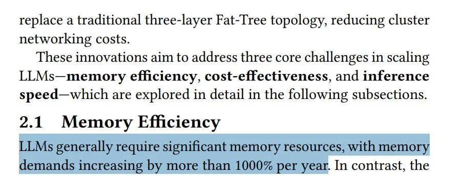
According to the paper, the number of parameters, context window length, and batch size in LLMs are increasing by nearly an order of magnitude each year. This is causing a rapid surge in memory requirements.
In other words, the pace of LLM development is far outstripping the pace of HBM technology development.
(2) Speed and Physical Limits of HBM Supply
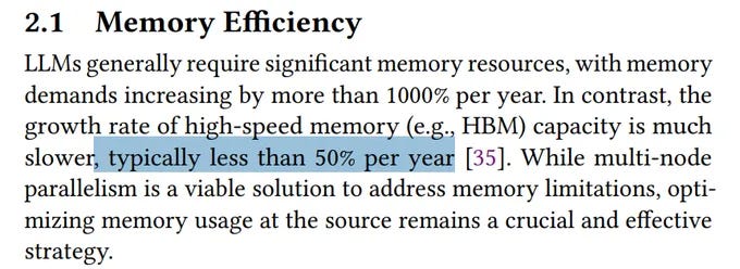
In contrast, HBM capacity is growing by less than 50% annually.
This means HBM manufacturers simply cannot keep up with the demands of models and data, indicating that the bottleneck for large-scale AI systems is naturally shifting more and more towards memory.
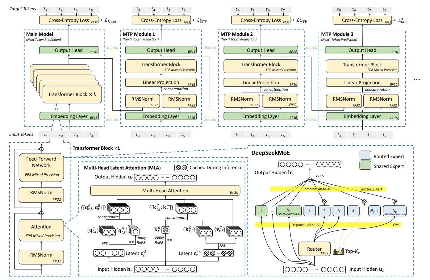
(3) Fundamental Limitations of Compression Techniques like MLA/FP8
The paper introduces various techniques to significantly reduce HBM usage per token, such as Multi-head Latent Attention (MLA) for KV cache optimization, low-precision quantization (FP8), and activation quantization.
MLA: Reduces memory usage by 4-5 times compared to conventional methods.
FP8: Halves memory usage compared to BF16.
Nevertheless, because the model size, number of tokens, and context length themselves are growing exponentially faster than the rate at which HBM usage per token is being reduced, the overall demand for HBM is inevitably bound to continue increasing.
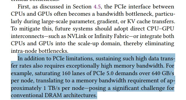
(4) The HBM Bottleneck in Real Data Center Environments
The paper emphasizes that in a real data center, HBM needs to become much faster (i.e., over 1TB/s) to fully saturate the 160 lanes of PCIe 6.0.
To meet this future demand, it suggests that:
Increasing the number of HBM stacks
Expanding the interposer size
Introducing new packaging methods like System-on-Wafer (SoW) will be necessary.

This will accelerate the high-value-add trend for HBM, as more expensive packaging and higher capacity HBM will be required.
In summary, my view is that HBM is the biggest bottleneck in AI development, and therefore, the high-value-add evolution of HBM is essential for future AI advancement.Now that you understand why HBM is important, let's move on to the specifics of HBM.
What has been the reason for SK hynix's success in the HBM space?
Of course, it's partly due to the windfall benefit from its competitor, Samsung, losing its edge through missteps.
However, what I want to emphasize is that SK hynix has been the sole HBM manufacturer collaborating with NVIDIA since HBM3.
Micron lost its lead in HBM by pushing a different standard called HMC, and Samsung disbanded its HBM team in 2019, citing a lack of profitability.
Consequently, only SK hynix consistently invested in HBM, which bore fruit with the HBM3 used in the H100, forging a strong relationship with NVIDIA that continues to this day.
Some might say that SK hynix's unique MR-MUF process is the reason for its current position, but I see it differently.
While it's true that MR-MUF yields are better than the TC-NCF used by Samsung and Micron, I have heard from industry insiders that this was not the deciding factor for NVIDIA's supply contracts.
Rather, it's Samsung's mistake in 2021—developing 1a, 1b, and 1c simultaneously—that has had a snowball effect to this day.
Let me summarize the situation at that time.
Under the direction of senior management, Samsung proceeded with the simultaneous development of 1a, 1b, and 1c nodes.
This was an extremely reckless move. Typically, DRAM node development is done sequentially: 1a → 1b → 1c.
This sequential process allows the know-how and technology from the previous node to be incorporated into the next, optimizing development resources.
However, Samsung's senior management was confident, believing their superior manpower and CAPA could handle it.
If only they had known this would be a disastrous decision with consequences felt to this day... As Samsung developed 1a, 1b, and 1c concurrently, errors occurred in all nodes, leading to heat and yield issues.
Yet, they transferred the flawed nodes directly to mass production lines and sold products made with these defective nodes for some time, claiming there were no problems.
However, as issues like the inability to overclock, high heat generation, and low yields driving up costs became apparent, Vice Chairman Jun Young-hyun, brought in as a relief pitcher, ordered a redesign of the nodes. It was like fixing the barn after the cow was stolen, but it was necessary. The foundational node had to be fixed to improve HBM and secure supply deals with NVIDIA.
So much for the internal affairs... You are aware that Samsung's HBM3E is made using the 1a node, right?
Internally, Samsung calls the redesigned 1a node "1ap," but we can move past that.
The reason Samsung's redesigned HBM3E is supplied to AMD and Broadcom but not to NVIDIA is simple.
Even with the redesign, it's still a 1a node, which remains inferior to the 1b nodes from SK hynix and Micron.
This means Samsung's HBM3E has worse power efficiency and higher heat generation compared to its competitors' HBM3E.
Based on my most recent information gathering, Samsung is reportedly considering abandoning the plan to supply HBM3E 12-stack to NVIDIA this year and is instead going all-in on HBM4.
If this happens, I believe the existing HBM3E 8-stack and 12-stack inventory could be recorded as a significant liability and loss for Samsung.
Despite this, there is still hope for Samsung.
Keep reading with a 7-day free trial
Subscribe to SemiconSam to keep reading this post and get 7 days of free access to the full post archives.